EasyManua.ls Logo

ST STM32F0 Series User Manual

ST STM32F0 Series
91 pages
To Next Page IconTo Next Page
To Previous Page IconTo Previous Page
Page #50 background image
The STM32 Cortex-M0 instruction set PM0215
50/91 Doc ID 022979 Rev 1
Examples
Multiword arithmetic examples
Specific example: 64-bit addition shows two instructions that add a 64-bit integer contained
in R0 and R1 to another 64-bit integer contained in R2 and R3, and place the result in R0
and R1.
Specific example: 64-bit addition
ADDS R0, R0, R2 ; add the least significant words
ADCS R1, R1, R3 ; add the most significant words with carry
Multiword values do not have to use consecutive registers. Specific example: 96-bit
subtraction shows instructions that subtract a 96-bit integer contained in R1, R2, and R3
from another contained in R4, R5, and R6. The example stores the result in R4, R5, and R6.
Specific example: 96-bit subtraction
SUBS R4, R4, R1 ; subtract the least significant words
SBCS R5, R5, R2 ; subtract the middle words with carry
SBCS R6, R6, R3 ; subtract the most significant words with carry
Specific example: Arithmetic negation shows the RSBS instruction used to perform a 1's
complement of a single register.
Specific example: Arithmetic negation
RSBS R7, R7, #0 ; subtract R7 from zero
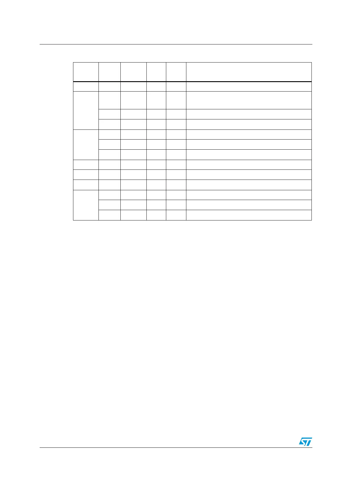
Table 20. ADCS, ADD, RSBS, SBCS and SUB operand restrictions
Instructi
on
Rd Rn Rm imm Restrictions
ADCS R0-R7 R0-R7 R0-R7 - Rd and
Rn must specify the same register.
ADD
R0-R15 R0-R15 R0-PC -
Rd and
Rn must specify the same register.
Rn and Rm must not both specify PC.
R0-R7 SP or PC - 0-1020 Immediate value must be an integer multiple of four.
SP SP - 0-508 Immediate value must be an integer multiple of four.
ADDS
R0-R7 R0-R7 - 0-7 -
R0-R7 R0-R7 - 0-255 Rd and
Rn must specify the same register.
R0-R7 R0-R7 R0-R7 - -
RSBS R0-R7 R0-R7 - - -
SBCS R0-R7 R0-R7 R0-R7 - Rd and
Rn must specify the same register.
SUB SP SP - 0-508 Immediate value must be an integer multiple of four.
SUBS
R0-R7 R0-R7 - 0-7 -
R0-R7 R0-R7 - 0-255 Rd and
Rn must specify the same register.
R0-R7 R0-R7 R0-R7 - -

Table of Contents

Other manuals for ST STM32F0 Series

Question and Answer IconNeed help?

Do you have a question about the ST STM32F0 Series and is the answer not in the manual?

ST STM32F0 Series Specifications

General IconGeneral
SeriesSTM32F0
CoreARM Cortex-M0
Operating FrequencyUp to 48 MHz
Flash Memory16 KB to 256 KB
SRAM4 KB to 32 KB
ADC Resolution12-bit
ADC ChannelsUp to 16
Operating Voltage2.0 V to 3.6 V
DAC Resolution12-bit (some series)
Communication InterfacesI2C, SPI, USART, USB, CAN
Operating Temperature-40°C to 85°C
Package OptionsLQFP, TSSOP, UFQFPN, WLCSP

Summary

Introduction to STM32F0xxx Programming

About this document

1.1 Typographical conventions

Defines typographical conventions used in the document.

1.2 List of abbreviations for registers

Lists abbreviations used for register descriptions.

1.3 About the STM32 Cortex-M0 processor and core peripherals

Overview of the Cortex-M0 processor and its core peripherals.

The STM32 Cortex-M0 processor

2.1 Programmers model

Describes the Cortex-M0 programmer's model, modes, and stacks.

2.2 Memory model

Details the processor memory map and memory access behavior.

2.3 Exception model

Explains the exception model, states, types, and priorities.

2.4 Fault handling

Covers fault handling mechanisms, including lockup states.

2.5 Power management

Describes sleep and deep sleep modes for power saving.

The STM32 Cortex-M0 instruction set

3.1 Instruction set summary

Summarizes the Thumb instruction set supported by the Cortex-M0.

3.4 Memory access instructions

Covers instructions for loading and storing data from/to memory.

3.5 General data processing instructions

Describes instructions for arithmetic, logical, and data manipulation operations.

3.6 Branch and control instructions

Details instructions for program flow control and branching.

Core peripherals

4.1 About the STM32 Cortex-M0 core peripherals

Introduces the core peripherals and their address map.

4.2 Nested vectored interrupt controller (NVIC)

Details the NVIC's support for interrupts and its registers.

4.3 System control block (SCB)

Describes the SCB for system implementation information and control.

4.4 SysTick timer (STK)

Explains the SysTick timer's functionality and registers.

Revision history

Related product manuals