EasyManua.ls Logo

ST STM32F0 Series User Manual

ST STM32F0 Series
91 pages
To Next Page IconTo Next Page
To Previous Page IconTo Previous Page
Page #89 background image
PM0215 Core peripherals
Doc ID 022979 Rev 1 89/91
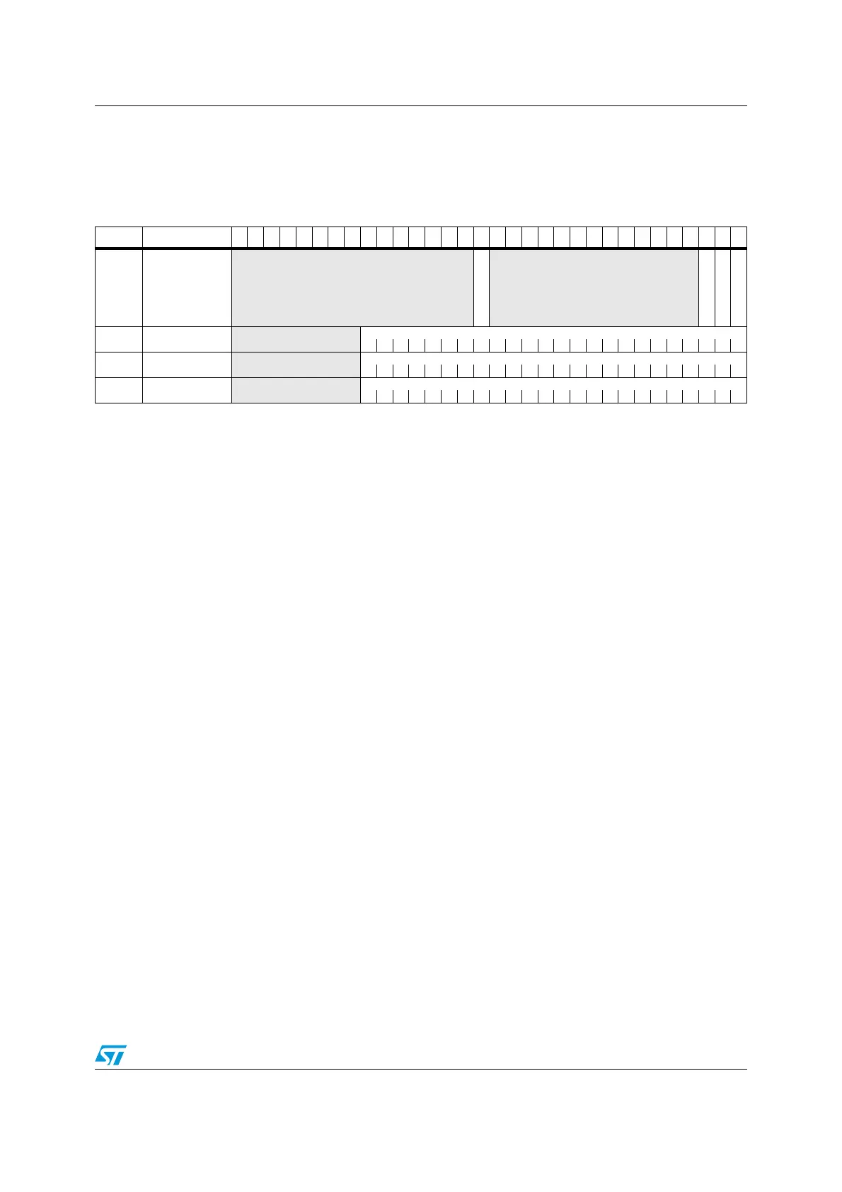
4.4.6 SysTick register map
The table provided shows the SysTick register map and reset values. The base address of
the SysTick register block is 0xE000 E010.
Table 34. SysTick register map and reset values
Offset Register
31
30
29
28
27
26
25
24
23
22
21
20
19
18
17
16
15
14
13
12
11
10
9
8
7
6
5
4
3
2
1
0
0x00
STK_CSR
Reserved
COUNTFLAG
Reserved
CLKSOURCE
TICK INT
EN ABLE
Reset Value 0 1 0 0
0x04
STK_RVR
Reserved
RELOAD[23:0]
Reset Value 000000000000000000000000
0x08
STK_CVR
Reserved
CURRENT[23:0]
Reset Value 000000000000000000000000
0x0C
STK_CALIB
Reserved
TENMS[23:0]
Reset Value 000000000000000000000000

Table of Contents

Other manuals for ST STM32F0 Series

Question and Answer IconNeed help?

Do you have a question about the ST STM32F0 Series and is the answer not in the manual?

ST STM32F0 Series Specifications

General IconGeneral
SeriesSTM32F0
CoreARM Cortex-M0
Operating FrequencyUp to 48 MHz
Flash Memory16 KB to 256 KB
SRAM4 KB to 32 KB
ADC Resolution12-bit
ADC ChannelsUp to 16
Operating Voltage2.0 V to 3.6 V
DAC Resolution12-bit (some series)
Communication InterfacesI2C, SPI, USART, USB, CAN
Operating Temperature-40°C to 85°C
Package OptionsLQFP, TSSOP, UFQFPN, WLCSP

Related product manuals