PM0215 Core peripherals
Doc ID 022979 Rev 1 71/91
4.2.2 Interrupt set-enable register (ISER)
Address offset: 0x00
Reset value: 0x0000 0000
The ISER register enables interrupts, and shows which interrupts are enabled
4.2.3 Interrupt clear-enable register (ICER)
Address offset: 0x080
Reset value: 0x0000 0000
The ICER register disables interrupts, and shows which interrupts are enabled.
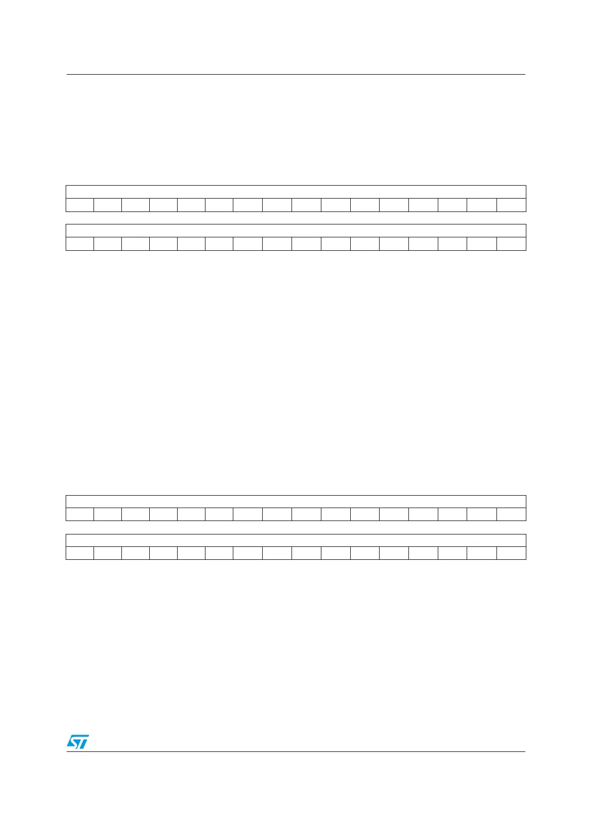
31 30 29 28 27 26 25 24 23 22 21 20 19 18 17 16
SETENA[31:16]
rs rs rs rs rs rs rs rs rs rs rs rs rs rs rs rs
1514131211109876543210
SETENA[15:0]
rs rs rs rs rs rs rs rs rs rs rs rs rs rs rs rs
Bits 31:0 SETENA: Interrupt set-enable bits.
Write:
0: No effect
1: Enable interrupt
Read:
0: Interrupt disabled
1: Interrupt enabled.
If a pending interrupt is enabled, the NVIC activates the interrupt based on its priority. If an
interrupt is not enabled, asserting its interrupt signal changes the interrupt state to pending,
but the NVIC never activates the interrupt, regardless of its priority.
31 30 29 28 27 26 25 24 23 22 21 20 19 18 17 16
CLRENA[31:16]
rc_w1 rc_w1 rc_w1 rc_w1 rc_w1 rc_w1 rc_w1 rc_w1 rc_w1 rc_w1 rc_w1 rc_w1 rc_w1 rc_w1 rc_w1 rc_w1
1514131211109876543210
CLRENA[15:0]
rc_w1 rc_w1 rc_w1 rc_w1 rc_w1 rc_w1 rc_w1 rc_w1 rc_w1 rc_w1 rc_w1 rc_w1 rc_w1 rc_w1 rc_w1 rc_w1
Bits 31:0 CLRENA: Interrupt clear-enable bits.
Write:
0: No effect
1: Disable interrupt
Read:
0: Interrupt disabled
1: Interrupt enabled.