MOSI1MISO1CS1CLK1
HOST
INTn
NRST
RS232
TX/RX
XDS110
CLK1 CS1 MISO1 MOSI1
HOST
INTn
NRST
RS232
TX/RX
FTDI
FT4232
CLK1
CS1
MISO1
MOSI1
HOST
INTn
NRST
RS232
TX/RX
SPI_CLK1
SPI_CS1
SPI_MISO1
SPI_MOSI1
HOST INTn
NRST
RS232
TX/RX
60 PIN
CONNECTOR
DCA1000
SCL SDA
GPIO[2:0]
NERR_IN
NERR_OUT
SOP[2:0]
CLK2/UART3
CS2/UART4
MISO2/SCL
MOSI2/SDA
CAN1 & 2
TX1
TX2
RX1
RX2
JTAG SIGNALS
FROM XDS110
14PIN
HEADER
DIP
SW
TMS/TCK/TDI
TDO SIGNALS
SOP[2:0]
NERR
IN/OUT
GPIO
[2:0]
CS2CLK2
2:1 MUX
40-PIN LP / BP HEADER
RS232
TX/RX
NRST
HOST
INTn
CLK1 CS1 MISO1 MOSI1
MISO2
/SCL
MOSI2
/SDA
SOP[2:0]
NERR
IN/OUT
GPIO
[2:0]
60 PIN HD CONNECTOR
MOSI2MISO2CS2CLK2
DIP
SW
SPI 2
SDA
SCL
2:1 MUX
2:1 MUX
2:1 MUX
2:1 MUX
2:1 MUX
2:1 MUX
JTAG SIGNALS
DIP
SW
RS232
TX/RX
2:1 MUX
DIP
SW
DIP
SW
DIP
SW
DIP
SW
DIP
SW
MMWAVEICBOOST
www.ti.com
10
SWRU546C–October 2018–Revised April 2020
Submit Documentation Feedback
Copyright © 2018–2020, Texas Instruments Incorporated
mmWaveICBoost and Antenna Module
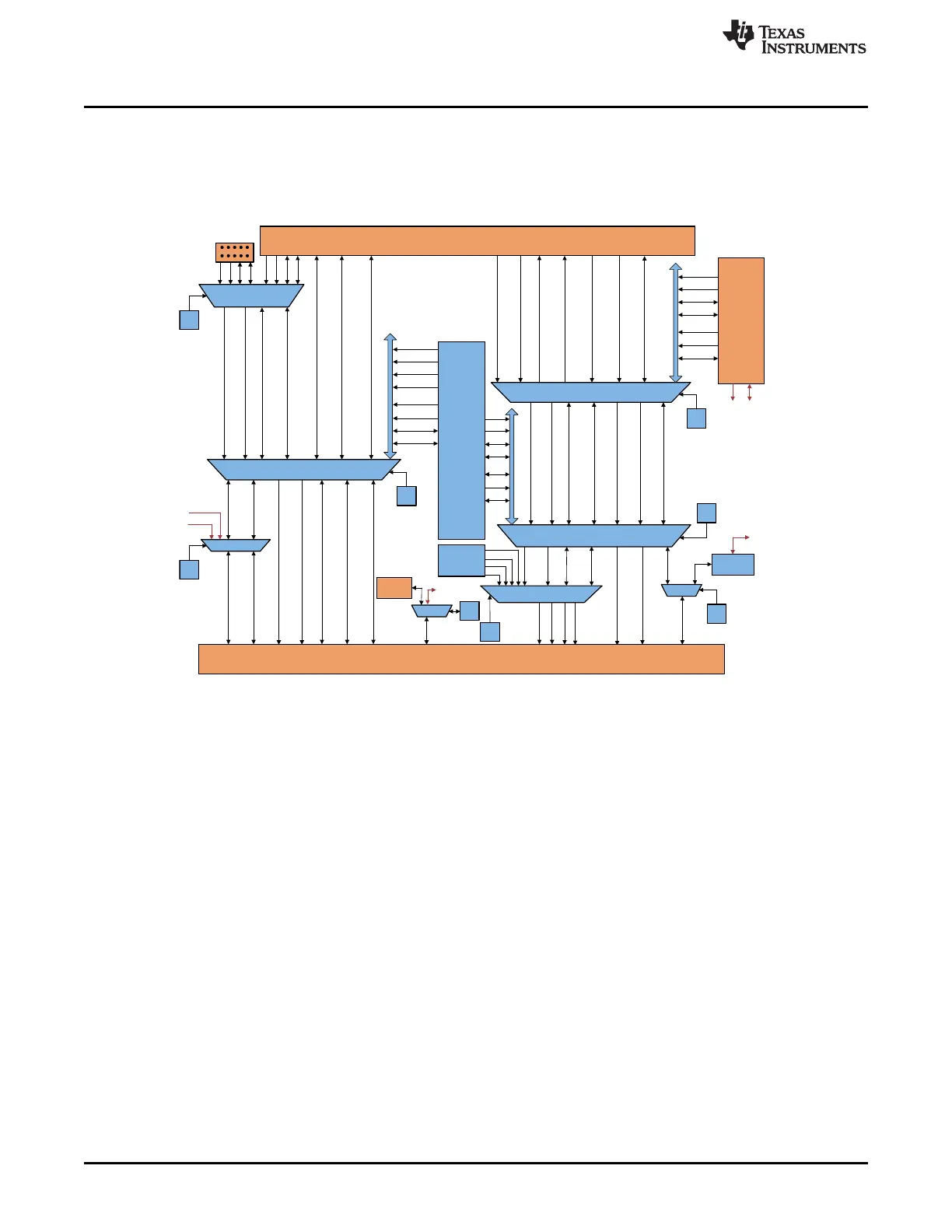
2.3 Muxing Scheme for Multiple Sources
There are multiple sources as shown in Figure 4 such as 40 pin LP/BP, DCA1000 EVM, onboard FTDI
and XDS110 that can control the Radar front-end chip in the starter kit. This is done with the help of mux
scheme implemented on the MMWAVEICBOOST. Follow the switch settings as shown in Table 1 to avoid
the conflicts. The most used configuration is the default position.
Figure 4. Muxing Scheme