www.ti.com
MMWAVEICBOOST
19
SWRU546C–October 2018–Revised April 2020
Submit Documentation Feedback
Copyright © 2018–2020, Texas Instruments Incorporated
mmWaveICBoost and Antenna Module
Table 5. J5 Connector Pinout
Pin Number Description Pin Number Description
1 3V3 2 5V
3 NC 4 GND
5 RS232 (TX from xWR device)
(1)
6 NC
7 RS232 (RX into xWR device)
(1)
8 NC
9 SYNC_IN 10 NC
11 NC 12 NC
13 SPI_CLK 14 PGOOD
(1)
15 GPIO0 16 PMIC_Enable
(3)
17 SCL 18 SYNC_OUT
19 SDA 20 PMIC CLKOUT
(1) When running the OOB demo, the RS232 TX and RX pins are used for user and configuration files. This is the same pin
connected to the XDS110 and displayed through the emulator as a Application/User UART COM port.
(2) Indicates that all the powers are stable in the standard LP/BP boards are stable, which enables or disables the power of FTDI
and XDS110 interfaces. A HIGH on the PGOOD signal (3.3 V) indicates the supply is stable. The I/Os of the front-end chip are
not safe to operate by the XDS110/FTDI before this I/O supply is stable, to avoid leakage current into the I/Os.
(3) Controls the PMIC enable for starter kits. The MCU can use this to shut down the PMIC and xWR device during the periods it
does not use the xWR device and save power. The power up of the PMIC takes approximately 5 ms once the enable signal is
made high.
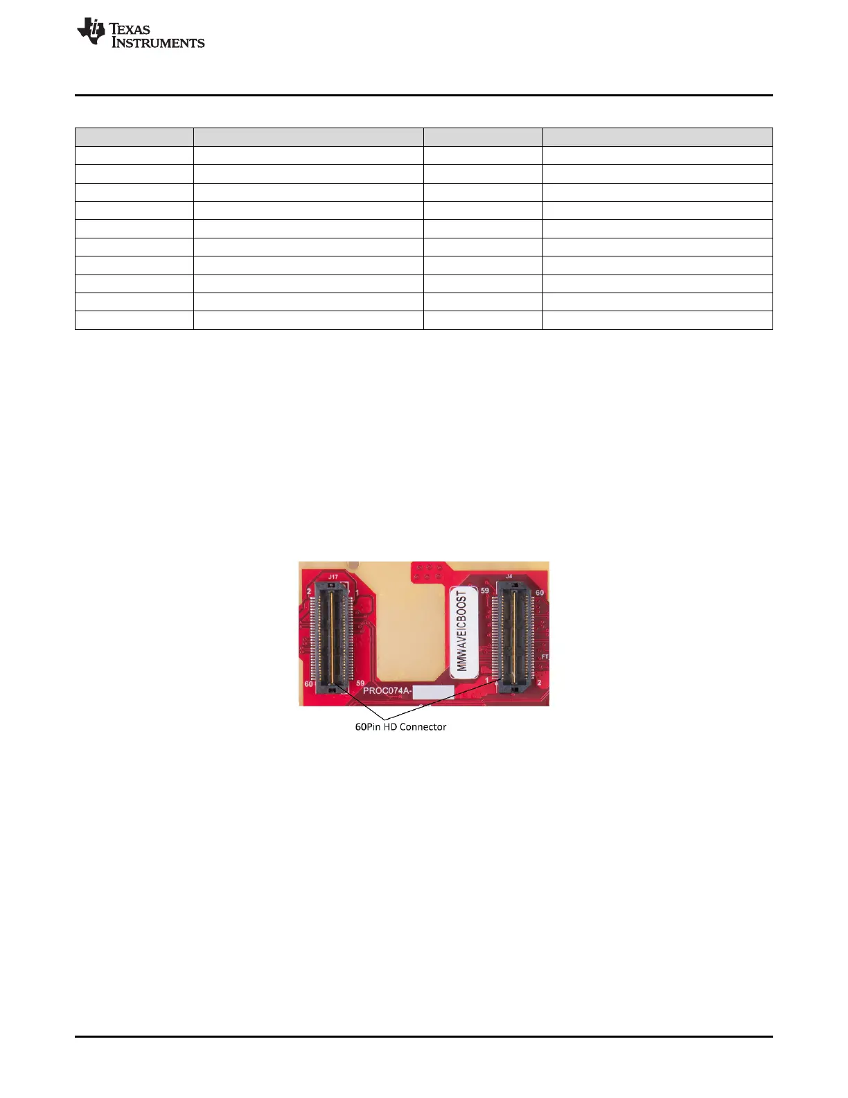
2.7.2 60-Pin High Density (HD) Connector (J4 and J17)
The 60-pin HD connector shown in Figure 18 provides the high-speed CSI/LVDS data, controls signals
(SPI, UART, I2C, NRST, NERR, and SOPs) and JTAG debug signals from the starter kit. The Trace and
DMM interface lines are also available through this connector.
Figure 18. 60-Pin HD Connectors