xWR6843ISK / IWR6843ISK-ODS REV C
www.ti.com
32
SWRU546C–October 2018–Revised April 2020
Submit Documentation Feedback
Copyright © 2018–2020, Texas Instruments Incorporated
mmWaveICBoost and Antenna Module
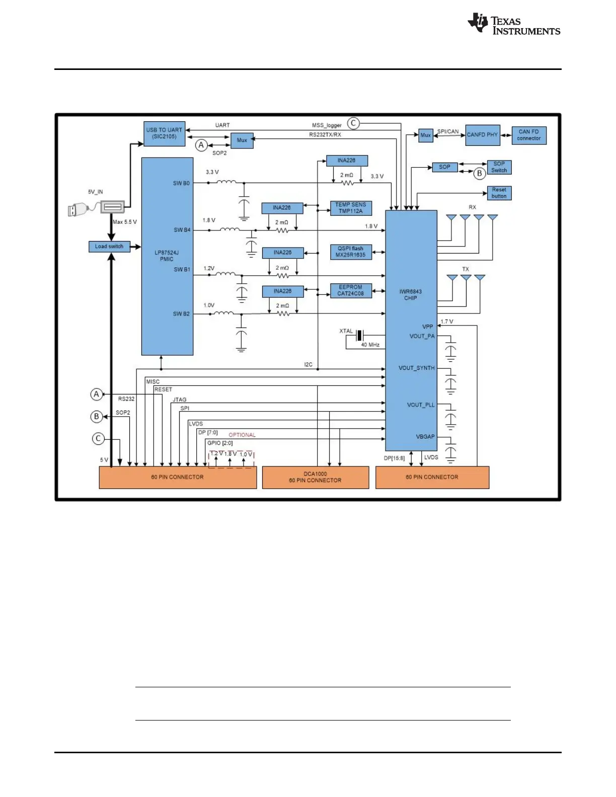
3.2 xWR6843ISK/IWR6843ISK-ODS Block Diagram
Figure 38 shows the functional block diagram.
Figure 38. Block Diagram of xWR6843ISK/IWR6843ISK-ODS
3.3 PCB Storage and Handling Recommendations
The immersion silver finish of the PCB provides a better high-frequency performance, but is also prone to
oxidation in open environments. This oxidation causes the surface around the antenna region to blacken.
To avoid oxidation, the PCB should be stored in an ESD cover and kept at a controlled room temperature
with low humidity conditions. All ESD precautions must be taken while using and handling the EVM.
3.4 Power Connections
The antenna module is powered by the 3.3 V from the 60-pin HD connectors. When power is supplied, an
on-board PMIC and LDO generate the voltages. The PGOOD LED glows to indicate all voltage rails are in
limits.
NOTE: After the 3.3-V supply is provided to the EVM, TI recommends toggling the NRST signal
once to ensure a reliable boot-up state; this signal is accessible on the 60-pin HD connector.