Chapter 8 Drawings
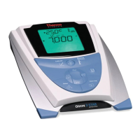
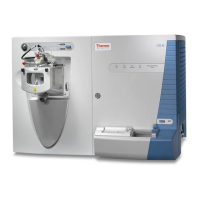
Figure 8.1 Spectronic GENESYS 10 Wiring Diagram ...............................................................................8-3
Figure 8.2 Keypad Schematic....................................................................................................................8-5
Figure 8.3 Main board CPU 1 of 14 ...........................................................................................................8-7
Figure 8.4 Main board Memory and Address Decode 2 of 14...................................................................8-9
Figure 8.5 Main board Printer, RS232, DAC Control, RTC 3 of 14 .........................................................8-11
Figure 8.6 Main board LCD Controller 4 of 14.........................................................................................8-13
Figure 8.7 Main board LCD Biasing Sequencing 5 of 14.........................................................................8-15
Figure 8.8 Main board tungsten Lamp Supply 6 of 14.............................................................................8-17
Figure 8.9 Main board grating motor Microstep Drive7 of 14 ..................................................................8-19
Figure 8.10 Main board turret and Filter motor Control 8 of 14 ...............................................................8-21
Figure 8.11 Main board Analog Front End 9 of 14...................................................................................8-23
Figure 8.12 Main board Delta Sigma A/D Converter10 of 14 ..................................................................8-25
Figure 8.13 Main board Detector Gain Select, Analog PWR Reg.11 of 14 .............................................8-27
Figure 8.14 Main board Flash lamp PWR+CNTL, 7V motor PWR 12 of 14 ............................................8-29
Figure 8.15 Main board Keypad Interface 13 of 14 .................................................................................8-31
Figure 8.16 Main board DC Power Entry and Filter14 of 14....................................................................8-33
Figure 8.17 Main board Block Diagram 1 of 2 .........................................................................................8-35
Figure 8.18 Memory Map 2 of 2...............................................................................................................8-37
Figure 8.19 Spectronic GENESYS 10 Detector board 1 of 3 ..................................................................8-39
Figure 8.20 Spectronic GENESYS 10 Detector board 2 of 3 ..................................................................8-41
Figure 8.21 Spectronic GENESYS 10 Detector board 3 of 3 ..................................................................8-43
Figure 8.22 Spectronic GENESYS 10 Analog Output Board...................................................................8-45
Figure 8.23 Spectronic GENESYS 6/Spectronic GENESYS 10 UVscanning Block Diagram.................8-47
Figure 8.24 Spectronic GENESYS 6/Spectronic GENESYS 10 UVscanning CPU.................................8-49
Figure 8.25 Spectronic GENESYS 6/Spectronic GENESYS 10 UVscanning Memory and Address Decode
..........................................................................................................................................................8-51
Figure 8.26 Spectronic GENESYS 6/Spectronic GENESYS 10 UVscanning Printer, RS232, and RTC.......
..........................................................................................................................................................8-53
Figure 8.27 Spectronic GENESYS 6/Spectronic GENESYS 10 UVscanning LCD Controller ................8-55
Figure 8.28 Spectronic GENESYS 6/Spectronic GENESYS 10 UVscanning LCD Bias Power Sequencing
..........................................................................................................................................................8-57
Figure 8.29 Spectronic GENESYS 6/Spectronic GENESYS 10 UVscanning Super I/O.........................8-59
Figure 8.30 Spectronic GENESYS 6/Spectronic GENESYS 10 UVscanning grating motor Micro-step
Drive
..................................................................................................................................................8-61
Figure 8.31 Spectronic GENESYS 6/Spectronic GENESYS 10 UVscanning turret and Filter motor Control
..........................................................................................................................................................8-63
Figure 8.32 Spectronic GENESYS 6/Spectronic GENESYS 10 UVscanning Analog Front End ............8-65
Figure 8.33 Spectronic GENESYS 6/Spectronic GENESYS 10 UVscanning Delta-Sigma A/D Converter ...
..........................................................................................................................................................8-67
Figure 8.34 Spectronic GENESYS 6/Spectronic GENESYS 10 UVscanning Detector Gain Select, Analog
Power Reg.
.......................................................................................................................................8-69
Figure 8.35 Spectronic GENESYS 6/Spectronic GENESYS 10 UVscanning Parallel Port ....................8-71
Figure 8.36 Spectronic GENESYS 6/Spectronic GENESYS 10 UVscanning Keypad Interface.............8-73
Figure 8.37 Spectronic GENESYS 6/Spectronic GENESYS 10 UVscanning Flash Lamp and DC Power
Entry
..................................................................................................................................................8-75
 Loading...