184 www.xilinx.com Virtex-5 RocketIO GTP Transceiver User Guide
UG196 (v1.3) May 25, 2007
Chapter 7: GTP Receiver (RX)
R
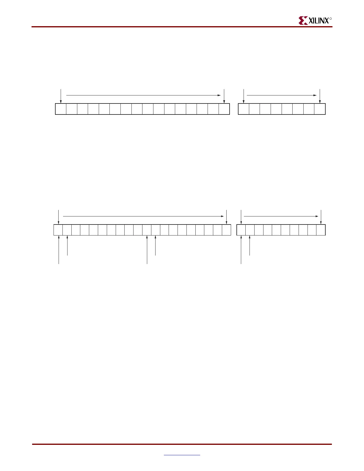
Figure 7-34 shows how RXDATA is received serially when the internal datapath is eight
bits (INTDATAWIDTH = 0) and 8B/10B decoding is disabled.
Figure 7-35 shows how RXDATA is received serially when the internal datapath is 10 bits
(INTDATAWIDTH = 1) and 8B/10B decoding is disabled. When RXDATA is 10 bits or 20
bits wide, the RXDISPERR and RXCHARISK ports are taken from the 8B/10B decoder
interface and are used to present the extra bits.
When 8B/10B decoding is used, the data interface is a multiple of 8 bits like in Figure 7-34,
but the data is decoded before it is presented at the RXDATA port. Refer to “Configurable
8B/10B Decoder,” page 157 for more details about bit ordering when using 8B/10B
decoding.
Connecting RXUSRCLK and RXUSRCLK2
The FPGA RX Interface includes two parallel clocks: RXUSRCLK and RXUSRCLK2.
RXUSRCLK is the internal clock for the PCS logic in the GTP receiver. The required rate for
RXUSRCLK depends on the internal datapath width of the GTP_DUAL tile
(INTDATAWIDTH), and the RX line rate of the GTP receiver (see “Serial In to Parallel Out
(SIPO),” page 141 to see how RX line rate is determined). Equation 7-7 shows how to
calculate the required rate for RXUSRCLK.
Equation 7-7
RXUSRCLK2 is the main synchronization clock for all signals into the RX side of the GTP
transceiver. Most signals into the RX side of the GTP receiver are sampled on the positive
edge of RXUSRCLK2. RXUSRCLK2 is the same rate at RXUSRCLK when RXDATAWIDTH
Figure 7-34: RX Interface with 8B/10B Bypassed (8-Bit Internal Datapath)
1514131211109876543210 76543210
RXDATAWIDTH = 1
INTDATAWIDTH = 0 and RXDEC8B10BUSE = 0
RXDATA
RXDATAWIDTH = 0
UG196_c7_31_100506
Received
Last
Received
Last
Received
First
Received
First
Figure 7-35: RX Interface with 8B/10B Bypassed (10-Bit Internal Datapath)
15141312111098 76543210 76543210
RXDATAWIDTH = 1
RXDATA
RXDATAWIDTH = 0
RXCHARISK[0]
RXDISPERR[0]
UG196_c7_32_100506
Received
Last
Received
Last
Received
First
Received
First
RXCHARISK[0]
RXDISPERR[0]
RXCHARISK[1]
RXDISPERR[1]
INTDATAWIDTH = 1 and RXDEC8B10BUSE = 0
RXUSRCLK Rate
Line Rate
Internal Datapath Width
-----------------------------------------------------------------=
 Loading...

