310 www.xilinx.com Virtex-5 RocketIO GTP Transceiver User Guide
UG196 (v1.3) May 25, 2007
Appendix E: Low Latency Design
R
GTP Receiver Latency
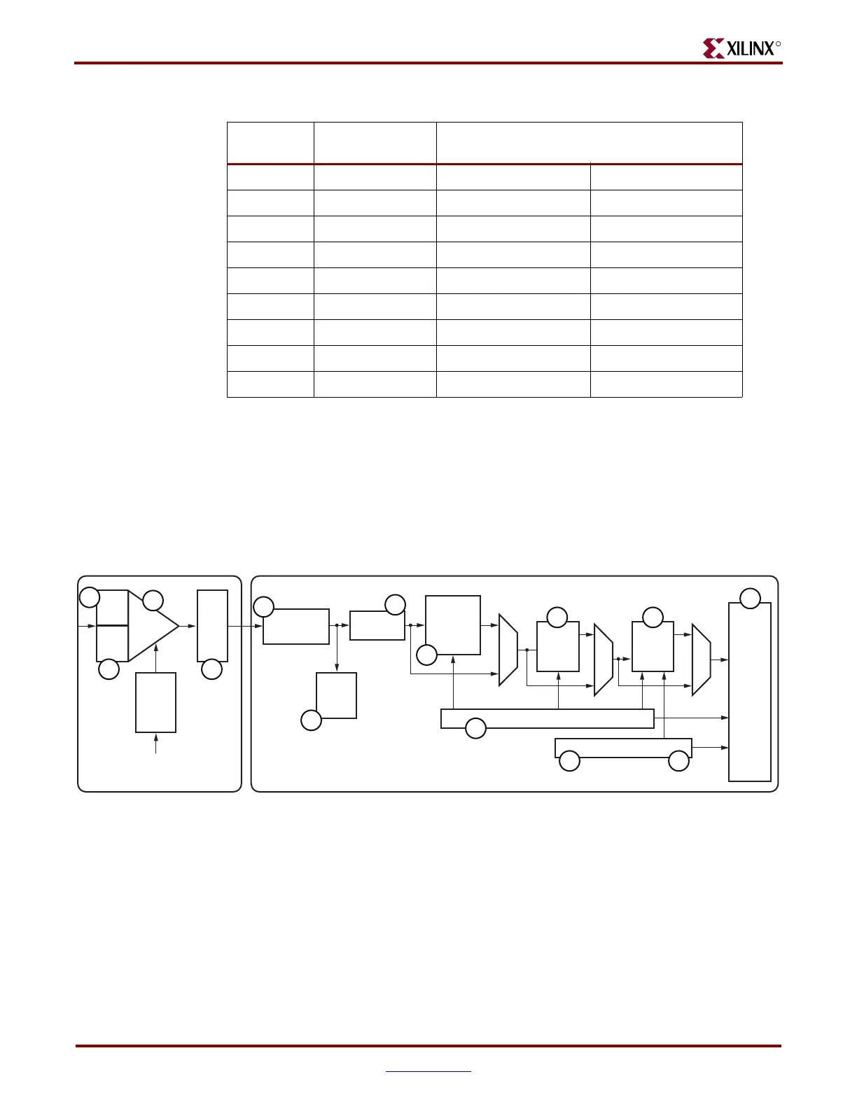
Figure E-2 shows a detailed block diagram of the GTP receiver. Refer to Chapter 7, “GTP
Receiver (RX),” and Figure 7-1, page 123 for more details on this figure and the GTP
receiver blocks.
Table E-2 defines the latency for the specific functional blocks or group of functional blocks
of the receiver section of the GTP transceiver. The values in the Block Number column
correspond to the circled numbers in Figure E-2.
Tab le E - 1 : GTP Transmitter Latency
Block
Number
Block Name Latency
TXDATAWIDTH = 0 TXDATAWIDTH = 1
1 Fabric Interface 1.5 cycles 2 cycles
TXENC8B10BUSE = 0 TXENC8B10BUSE = 1
2 8B/10B Encoder 0 cycles 1 cycle
TX_BUFFER_USE = 0 TX_BUFFER_USE = 1
3 TX FIFO 1 cycle 1-5 cycles
4+6+7+8+9 PMA + Interface 2 ± 0.5 cycles
Total Latency Max Min
10.5 cycles 4 cycles
Notes:
1. 1 cycle = 1 clock cycle at the TXUSRCLK rate.
Figure E-2: GTP RX Block Diagram
RX-PMA RX-PCS
From Shared PMA PLL
Rx
EQ
Rx
OOB
SIPO
10B/8B
Decoder
FPGA
RX
Interface
RX
Polarity
Over-
sampling
Loss of Sync
Rx Status Control
UG196_c7_01_041907
PRBS
Check
Rx
CDR
Shared
PMA
PLL
Divider
Comma
Detect
and
Align
Elastic
Buffer
1
3
2 4
5
7
6
8
9
12 13
10 11
14
 Loading...

