Virtex-5 RocketIO GTP Transceiver User Guide www.xilinx.com 207
UG196 (v1.3) May 25, 2007
REFCLK Guidelines
R
REFCLK Guidelines
Overview
This section focuses on the selection of the reference clock source or oscillator. An oscillator
is characterized by:
• Frequency range
• Output voltage swing
• Jitter (deterministic, random, peak-to-peak)
• Rise and fall times
• Supply voltage and current
• Noise specification
• Duty cycle and duty-cycle tolerance
• Frequency stability
These characteristics are selection criteria when choosing an oscillator for a GTP
transceiver design.
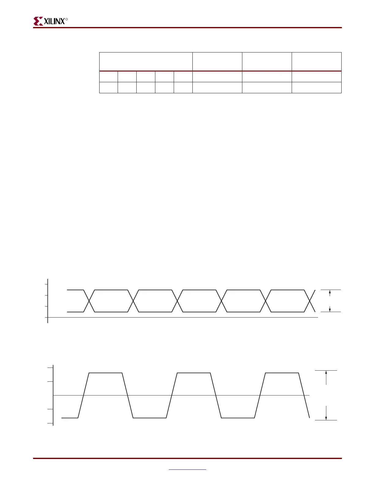
Figure 10-6 illustrates the convention for the single-ended clock input voltage swing, peak-
to-peak as used in the GTP transceiver portion of the Virtex-5 Data Sheet.
Figure 10-7 illustrates the differential clock input voltage swing, peak-to-peak, which is
defined as MGTREFCLKP – MGTREFCLKN.
1 1 1 1 0 39.9 49.8 29.9
1 1 1 1 1 39.1 48.8 29.3
Table 10-3: TERMINATION_CTRL Attribute Encoding (Continued)
TERMINATION_CTRL [4:0]
Nominal
Resistance [Ω]
+25% Resistance
[Ω]
-25% Resistance
[Ω]
Figure 10-6: Single-Ended Clock Input Voltage Swing, Peak-to-Peak
0
+V
MGTREFCLKP
MGTREFCLKN
V
ISE
UG196_c10_06_110206
Figure 10-7: Differential Clock Input Voltage Swing, Peak-to-Peak
0
+V
–V
MGTREFCLKP – MGTREFCLKN
V
IDIFF
UG196_c10_07_110206
 Loading...

