Virtex-5 RocketIO GTP Transceiver User Guide www.xilinx.com 89
UG196 (v1.3) May 25, 2007
R
Chapter 6
GTP Transmitter (TX)
This chapter shows how to configure and use each of the functional blocks inside the GTP
transmitter.
Transmitter Overview
Each GTP transceiver in the GTP_DUAL tile includes an independent transmitter, made
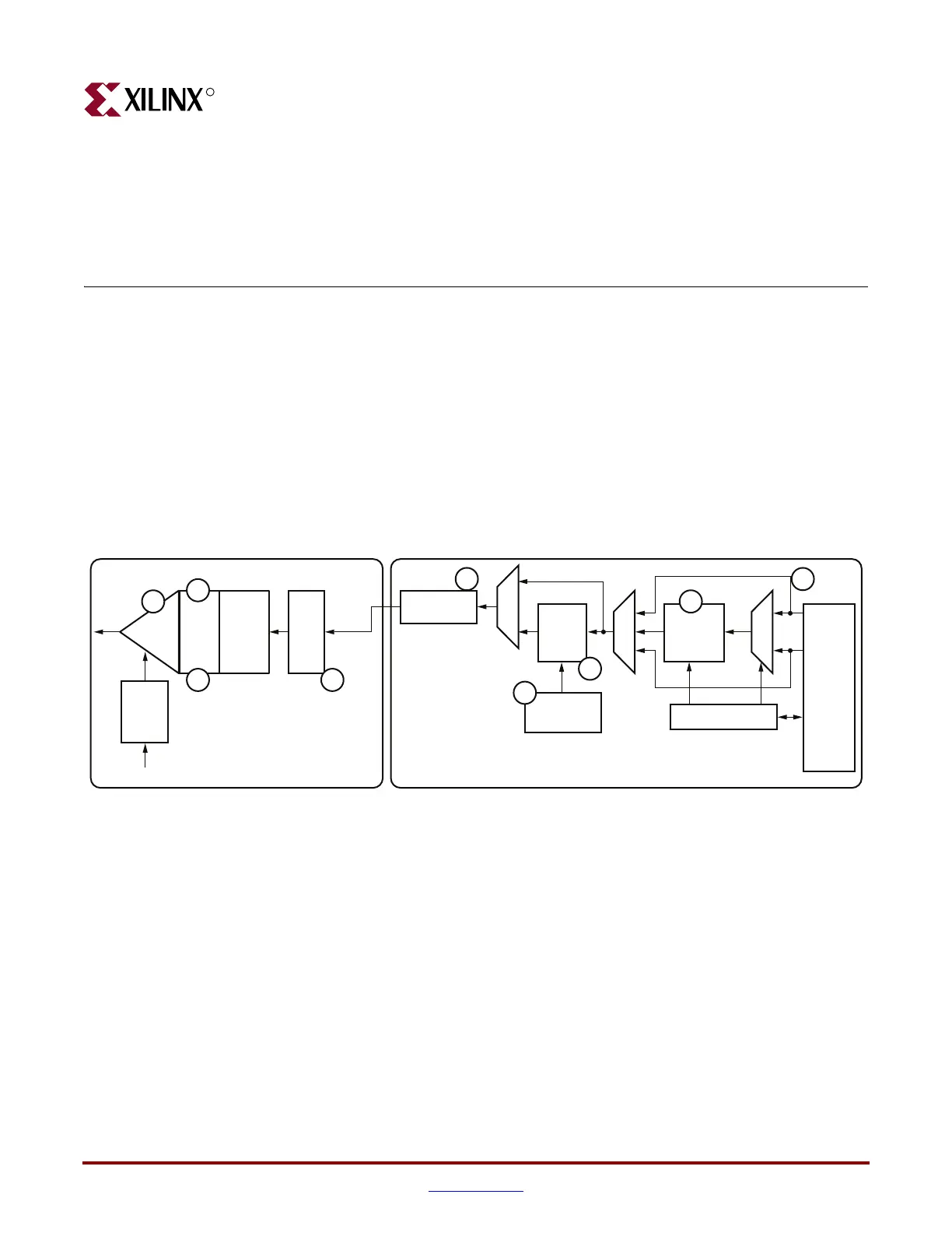
up of a PCS and a PMA. Figure 6-1 shows the functional blocks of the transmitter. Parallel
data flows from the FPGA into the FPGA TX interface, through the PCS and PMA, and
then out the TX driver as high-speed serial data. Refer to Appendix E, “Low Latency
Design,” for latency information on this block diagram.
The key elements within the GTP transmitter are:
1. “FPGA TX Interface,” page 90
2. “Configurable 8B/10B Encoder,” page 98
3. “TX Buffering, Phase Alignment, and Buffer Bypass,” page 102
4. “TX Polarity Control,” page 108
5. “TX PRBS Generator,” page 109
6. “Parallel In to Serial Out (PISO),” page 110
7. “Configurable TX Driver,” page 112
8. “PCI Express Receive Detect Support,” page 116
9. “TX OOB/Beacon Signaling,” page 119
Figure 6-1: GTP TX Block Diagram
TX-PMA TX-PCS
TX
Driver
TX PIPE Control
From Shared PMA PLL
TX
Preemp
PISO
Phase
Adjust
FIFO
8B/10B
Encoder
FPGA
TX
Interface
Polarity
Control
PRBS
Generator
UG196_c6_01_042407
Shared
PMA
PLL
Divider
TX
OOB
&
PCI
1
2
3
5
4
7
9
68
 Loading...

