2.7 – DDG™ SPECIFICATIONS
Gate pulse delay & width
•Adjustable from 0 ns to 10 s in 10 ps steps
•Software controlled, pre-programmed or real-time
TRIGGER OUTPUTS
Output A, B and C
•3x output, +5V CMOS level with 50 Ω source impedance; can drive 5V into a non-terminating load or
2.5V into 50 Ω load; output synchronized triggers for auxiliary equipment, e.g. lasers, ash lamps, or National
Instrument™ hardware
•Individual delays control from 0 ns to 10 s in 10 ps steps
•Congurable polarity
•Software controlled, pre-programmed or real-time
Fire •5V CMOS level reference signal for beginning and end of individual CCD exposure
Arm monitor
•5V CMOS level reference signal to indicate when system is ready to accept external triggers. Signal goes high
when system is ready to accept external triggers (after a complete readout has nished) including keep clean
and goes low when the exposure is nished
Gate & output A, B and C jitter •35 ps rms (relative to external trigger signal)
TRIGGER INPUTS
External trigger
•Trigger input for CCD and Digital Delay Generator
•Up to 500 kHz for Integrate-On-Chip mode
•Software-congurable polarity, termination and trigger threshold
•Fast external software option for most rapid camera response to external trigger (CCD keep clean interruption)
– no need for pre-trigger pulse
Direct gate •TTL input for exact external control of photocathode width and timing with smallest insertion delay.
ADDITIONAL CONTROLS
Gate monitoring •AC coupling from photocathode to monitor exact photocathode On/Off switching and timings
Insertion delay •< 19 ns in direct gate operation
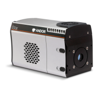
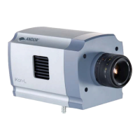
Introduction to the New iStar