— 61 —
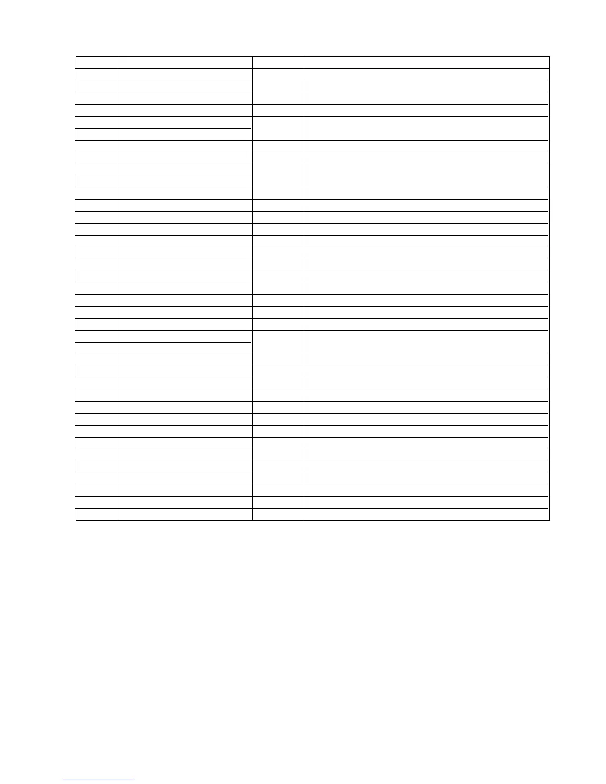
NO. PIN NAME I/O DESCRIPTION
219 AUDSYNC – AUD sync
220 AUDCK – AUD clock
221 VDDQ Power IO VDD
222 VSSQ Power IO GND
223 AUDATA0
– AUD data
224 AUDATA1
225 VDD Power Internal VDD
226 VSS Power Internal GND
227 AUDATA2
– AUD data
228 AUDATA3
229 Reserved – Do not connect
230 MD3/CE2A I/O Mode/PCMCIA-CE
231 MD4/CE2B I/O Mode/PCMCIA-CE
232 MD5 I Mode MD5
233 VDDQ Power IO VDD
234 VSSQ Power IO GND
235 DACK0 O DMAC0 bus acknowledge
236 DACK1 O DMAC1 bus acknowledge
237 DRAK0 O DMAC0 request acknowledge
238 DRAK1 O DMAC1 request acknowledge
239 VDD Power Internal VDD
240 VSS Power Internal GND
241 STATUS0
O Status
242 STATUS1
243 DREQ0 I Request from DMAC0
244 DREQ1 I Request from DMAC1
245 ASEBRK/BRKACK I/O Pin break/acknowledge (H-UDI)
246 TDO O Data out (H-UDI)
247 VDDQ Power IO VDD
248 VSSQ Power IO GND
249 VDD-PLL2 Power PLL2 VDD
250 VSS-PLL2 Power PLL2 GND
251 VDD-PLL1 Power PLL1 VDD
252 VSS-PLL1 Power PLL1 GND
253 VDD-CPG Power CPG VDD
254 VSS-CPG Power CPG GND
255 XTAL O Crystal resonator
256 EXTAL I External input clock/crystal resonator
I: Input
O: Output
I/O: Input/output
Power: Power supply
Notes: 1. Except in hardware standby mode, supply power to all power pins. In hardware standby mode, supply power to RTC as a
minimum.
2. Power must be supplied to VDD-PLL1/2 and VSS-PLL1/2 regardless of whether or not the on-chip PLL circuits are used.
3. Power must be supplied to VDD-CPG and VSS-CPG regardless of whether or not the on-chip crystal resonator is used.
4. Power must be supplied to VDD-RTC and VSS-RTC regardless of whether or not the on-chip RTC is used.
5. For the handling of the PCI bus pins in PCI-disabled mode, see table D.4 in appendix D.
* I/O attribute is I/O when used as a port.

 Loading...