2-10
Chadwick-Helmuth Company, Inc.
Chapter 2
- Overview and Basic Theory
2.3 System Architecture
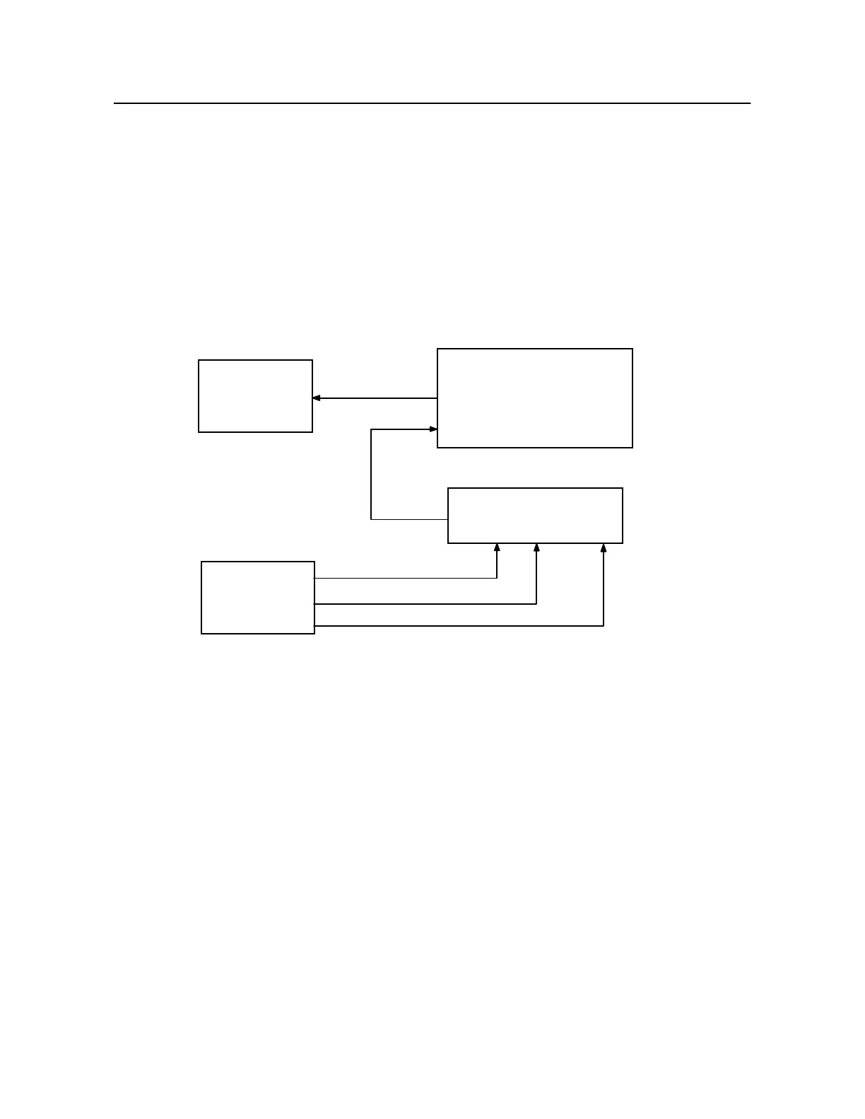
Figur e2-7 below shows an overall block diagram for the 8500C/C+ system. The 8500C/C+ itself can
be divided into the following major logical components:
• Digital subsystem, containing memory, microprocessor, communications controllers, and clock
chips
• Data acquisition or analog subsystem, containing analog inputs, waveform generator, input
multiplexor, analog-to-digital converter, programmable gain stage, antialiasing filter, and clip
detector
Figure 2-7. 8500C/C+ System Block Diagram
2.3.1 Digital Subsyste
The 8500C/C+ digital subsystem is made up of eight major functional blocks, as depicted in the block
diagram in Figur e2-8 on pag e2-11. All components communicate over a high-speed system bus, with
each block controlling its peripherals directly through dedicated interfaces.
Model 8500C/C+
Balancer/Analyzer
Main Unit
Strobex
28 VDC
Model 8520C
Signal Selector
Aircraft
Under Test
28 VDC
Vibration Input
Magnetic/Photocell Pickup Input
28 VDC
Signals
8500SYBK.DS4