18 UART
S1C17624/604/622/602/621 TECHNICAL MANUAL
Seiko Epson Corporation
18-7
If other interrupt conditions are satisfied, an interrupt occurs. You can inspect the PER, FER, and OER flags in
the UART interrupt handler routine to determine whether the UART interrupt was caused by a receive error. If
any of the error flags has the value 1, the interrupt handler routine will proceed with error recovery.
For more information on interrupt processing, see the “Interrupt Controlle
r (ITC)” chapter.
IrDA Interface18.8
This UART module includes an RZI modulator/demodulator circuit enabling implementation of IrDA 1.0-compatible
infrared communication function simply by adding basic external circuits.
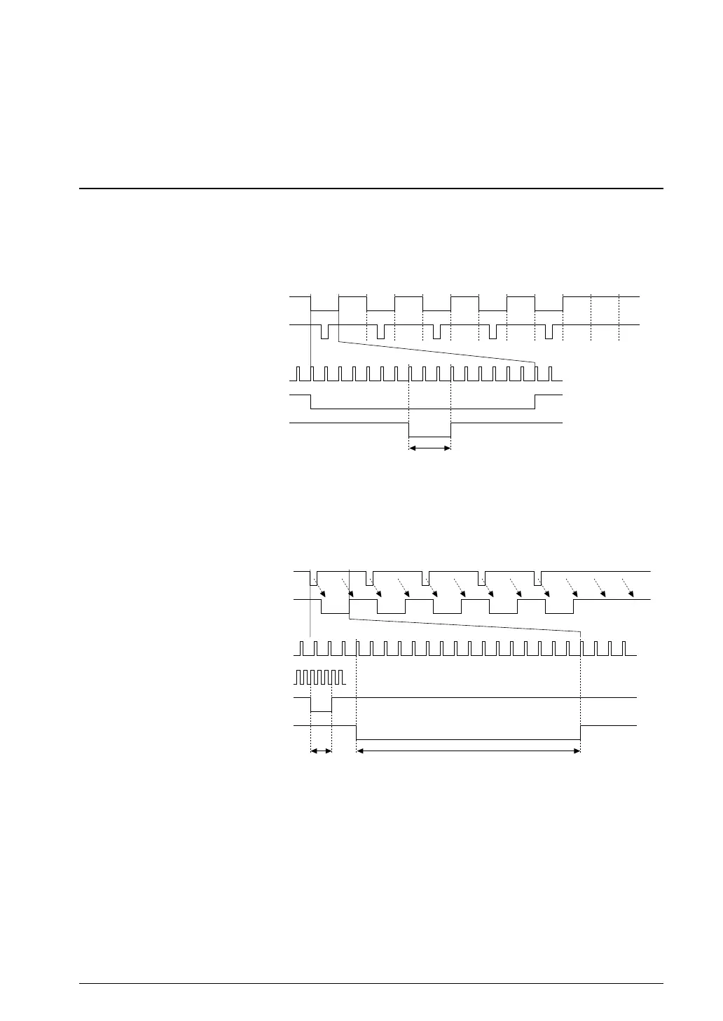
The transmit data output from the UART transmit shift register is input to the modulator circuit and output from the
SOUTx pin after the Low pulse has been modulated to a 3 × sclk1
6 cycle.
sclk16
Modulator input (shift register output)
Modulator output (SOUTx)
12389101116
3 × sclk16
Modulator input (shift register output)
Modulator output (SOUTx)
S1 D0 D1 D2 D3 D4 D5 D6 D7 PS2S3
(S1: Start bit, S2 & S3: Stop bits, P: Parity bit)
8.1 Transmission Signal WaveformFigure 18.
The received IrDA signal is input to the demodulator circuit and the Low pulse width is converted to 16 × sclk16
cycles before entry to the receive shift register. The demodulator circuit uses the pulse detection clock selected
separately from the transfer clock to detect Low pulses input (when minimum pulse width = 1.41 µs/115,200 bps).
(S1: Start bit, S2 & S3: Stop bits, P: Parity bit)
sclk16
irclk
Demodulator input (SINx)
Demodulator output (shift register input)
1 234 16
16 × sclk162 × irclk or more
Demodulator input (SINx)
Demodulator output (shift register input)
S1 D0 D1 D2 D3 D4 D5 D6 D7 PS2S3
8.2 Receive Signal WaveformFigure 18.
IrDA enable
To use the IrDA interface function, set IRMD/UART_EXPx register to 1. This enables the RZI modulator/de-
modulator circuit.
Note: This setting must be performed before setting other UART conditions.
IrDA receive detection clock selection
The input pulse detection clock is generated by dividing PCLK. The division ratio can be selected using IR-
CLK[2:0]/UA
RT_EXPx register.



 To Next Page