23 LCD DRIVER (LCD)
S1C17624/604/622/602/621 TECHNICAL MANUAL
Seiko Epson Corporation
23-15
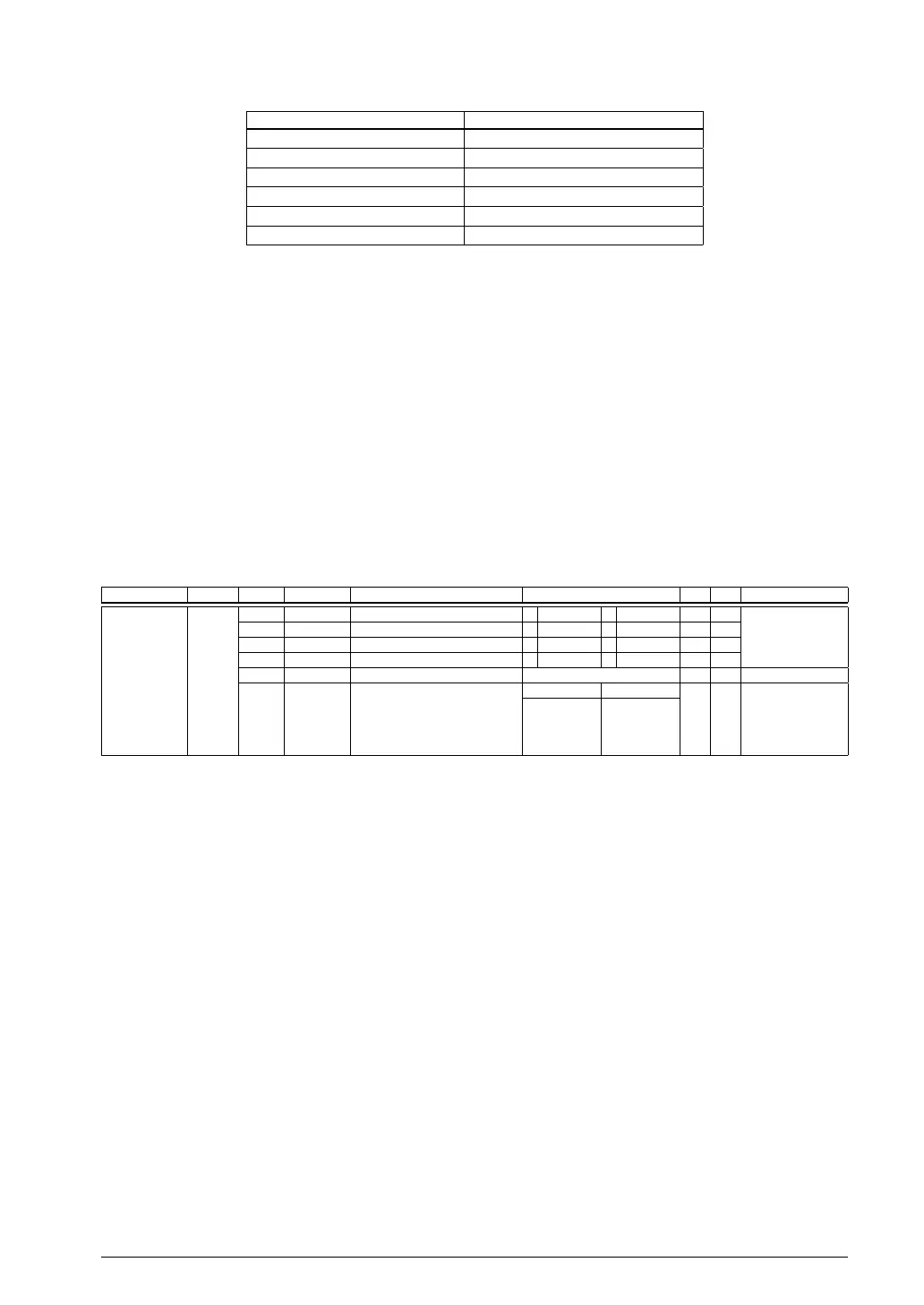
8.2 HSCLK Division Ratio SelectionTable 23.
LCKDV[2:0] Division ratio
0x7–0x5 Reserved
0x4 1/512
0x3 1/256
0x2 1/128
0x1 1/64
0x0 1/32
(Default: 0x0)
No division ratio needs to be selected if OSC1 is selected as the LCD clock source.
D1 LCKSRC: LCD Clock Source Select Bit
Selects the LCD clock source.
1 (R/W): OSC1 (default)
0 (R/W): HSCLK (IOSC or OSC3)
D0 LCKEN: LCD Clock Enable Bit
Enables or disables the LCD clock supply to the LCD driver.
1 (R/W): Enabled (on)
0 (R/W): Disabled (off) (default)
The LCKEN default sett
ing is 0, which stops the clock. Setting LCKEN to 1 feeds the clock selected as
above to the LCD driver. If no LCD display is required, stop the clock to reduce current consumption.
LCD Display Control Register (LCD_DCTL)
Register name Address Bit Name Function Setting Init. R/W Remarks
LCD Display
Control Register
(LCD_DCTL)
0x50a0
(8 bits)
D7
SEGREV
Segment output assignment control
1 Normal 0 Reverse 1 R/W
D6
COMREV
Common output assignment control
1 Normal 0 Reverse 1 R/W
D5
DSPAR
Display memory area control 1 Area 1 0 Area 0 0 R/W
D4
DSPREV
Reverse display control 1 Normal 0 Reverse 1 R/W
D3–2
–
reserved – – – 0 when being read.
D1–0
DSPC[1:0]
LCD display control DSPC[1:0] Display 0x0 R/W
0x3
0x2
0x1
0x0
All off
All on
Normal display
Display off
D7 SEGREV: Segment Output Assignment Control Bit
Inverts memory assignments for SEG pins.
1 (R/W): Norm
al (default)
0 (R/W): Inverted
When SEGREV is set to 1 (default), memory addresses are assigned to SEG pins in ascending order.
When SEGREV is set to 0, memory addresses are assigned to SEG pins in descending order. (See Fig-
ures 23.5.1 to 23.5.10.)
D6 COMREV: Common Output Assignment Control Bit
Inverts memory assignments for COM pins.
1 (R/W): Normal (default)
0 (R/W): Inverted
When COMREV is set to 1 (default), memory bits are assigned to C
OM pins in ascending order. When
COMREV is set to 0, memory bits are assigned to COM pins in descending order. (See Figures 23.5.1
to 23.5.10.)
D5 DSPAR: Display Memory Area Control Bit
Selects the display area.
1 (R/W): Display area 1
0 (R/W): Display area 0 (default)
 Loading...