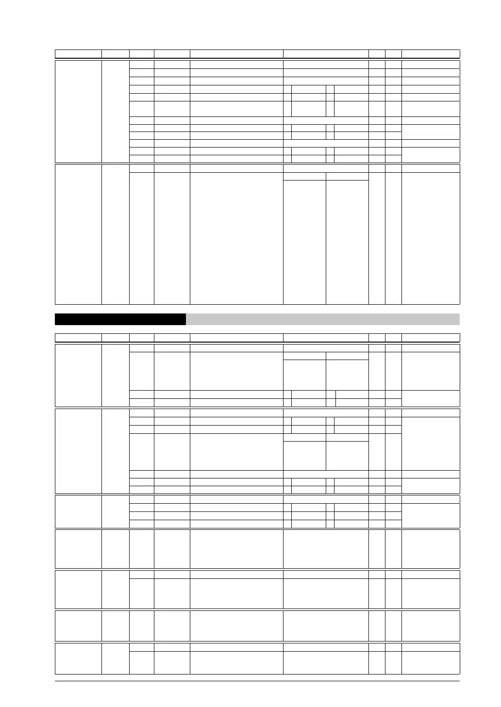
APPENDIX A LIST OF I/O REGISTERS
S1C17624/604/622/602/621 TECHNICAL MANUAL
Seiko Epson Corporation
AP-A-25
Register name Address Bit Name Function Setting Init. R/W Remarks
A/D Control/
Status Register
(ADC10_CTL
)
0x5384
(16 bits)
D15
–
reserved – – – 0 when being read.
D14–12
ADICH[2:0]
Conversion channel indicator 0x0 to 0x7 0x0 R
D11
–
reserved – – – 0 when being read.
D10
ADIBS
ADC10 status 1 Busy 0
Idle
0 R
D9
ADOWE
Overwrite error flag 1 Error 0 Normal 0 R/W Reset by writing 1.
D8
ADCF
Conversion completion flag 1 Completed 0 Run/Stand-
by
0 R Reset when ADC10_
ADD is read.
D7–6
–
reserved – – – 0 when being read.
D5
ADOIE
Overwrite error interrupt enable 1 Enable 0 Disable 0 R/W
D4
ADCIE
Conversion
completion int. enable 1 Enable 0 Disable 0 R/W
D3–2
–
reserved – – – 0 when being read.
D1
ADCTL
A/D conversion control 1 Start 0 Stop 0 R/W
D0
ADEN
ADC10 enable 1 Enable 0 Disable 0 R/W
A/D Clock
Control Register
(ADC_DIV)
0x5386
(16 bits)
D15–4
–
reserved – – – 0 when being read.
D3–0
ADDF[3:0]
A/D converter clock division ratio
select
ADDF[3:0]
Division ratio 0x0 R/W Source clock = PCLK
0xf
0xe
0xd
0xc
0xb
0xa
0x9
0x8
0x7
0x6
0x5
0x4
0x3
0x2
0x1
0x0
reserved
1/32768
1/16384
1/8192
1/4096
1/2048
1/1024
1/512
1/256
1/128
1/64
1/32
1/16
1/8
1/4
1/2
0x5067, 0x53a0–0x53ae R/F Converter
Register name Address Bit Name Function Setting Init. R/W Remarks
RFC Clock
Control Register
(OSC_RFC)
0x5067
(8 bits)
D7–4
–
reserved – – – 0 when being read.
D3–2
RFTCKDV
[1:0]
RFC clock division ratio select
RFTCKDV[1:0]
Division ratio 0x0 R/W When the clock
source is HSCLK
0x3
0x2
0x1
0x0
1/8
1/4
1/2
1/1
D1
RFTCKSRC
RFC clock source select 1 OSC1 0 HSCLK 1 R/W
D0
RFTCKEN
RFC clock enable 1 Enable 0 Disable 0 R/W
RFC Control
Register
(RFC_CTL
)
0x53a0
(16 bits)
D15–8
–
reserved – – – 0 when being read.
D7
CONEN
Continuous oscillation enable
1 Enable 0 Disable 0 R/W
D6
EVTEN
Event counter mode enable 1 Enable 0 Disable 0 R/W
D5–4
SMODE[1:0]
Sensor oscillation mode select
SMODE[1:0]
Sensor 0x0 R/W
0x3
0x2
0x1
0x0
reserved
DC capacitive
AC resistive
DC resistive
D3–2
–
reserved – – – 0 when being read.
D1
CHSEL
Conversion channel select
1 Ch.1 0 Ch.0 0 R/W
D0
RFCEN
RFC enable 1 Enable 0 Disable 0 R/W
RFC Oscillation
Trigger Register
(RFC_TRG
)
0x53a2
(16 bits)
D15–3
–
reserved – – – 0 when being read.
D2
SSENB
Sensor B oscillation control/status
1 Start/Run 0 Stop 0 R/W
D1
SSENA
Sensor A oscillation control/status
1 Start/Run 0 Stop 0 R/W
D0
SREF
Reference oscillation control/status
1 Start/Run 0 Stop 0 R/W
RFC
Measurement
Counter Low
Register
(RFC_MCL)
0x53a4
(16 bits)
D15–0
MC[15:0]
Measurement counter low-order
16-bit data
0x0–0xffff 0x0 R/W
RFC
Measurement
Counter High
Register
(RFC_MCH)
0x53a6
(16 bits)
D15–8
–
reserved – – – 0 when being read.
D7–0
MC[23:16]
Measurement counter high-order
8-bit data
0x0–0xff 0x0 R/W
RFC Time Base
Counter Low
Register
(RFC_TCL)
0x53a8
(16 bits)
D15–0
TC[15:0]
Time base counter low-order 16-
bit data
0x0–0xffff 0x0 R/W
RFC Time Base
Counter High
Register
(RFC_TCH)
0x53aa
(16 bits)
D15–8
–
reserved – – – 0 when being read.
D7–0
TC[23:16]
Time base counter high-order
8-bit data
0x0–0xff 0x0 R/W



 To Next Page