3 MEMORY MAP
3-8
Seiko Epson Corporation
S1C17624/604/622/602/621 TECHNICAL MANUAL
• 8-bit timers (T8F, 16-bit device)
• 16-bit timers (T16, 16-bit device)
• Interrupt controller (ITC, 16-bit device)
• SPI (SPI, 16-bit device)
• I
2
C master (I2CM, 16-bit device)
• I
2
C slave (I2CS, 16-bit device)
Internal Peripheral Area 2 (0x5000–)3.5.2
The internal peripheral area 2 beginning with address 0x5000 contains the I/O memory for the peripheral functions
listed below and this area can be ac
cessed in one cycle.
• Clock timer (CT, 8-bit device)
• Stopwatch timer (SWT, 8-bit device)
• Watchdog timer (WDT, 8-bit device)
• Clock generator (CLG, 8-bit device)
• LCD driver (LCD, 8-bit device)
• 8-bit OSC1 timer (T8OSC1, 8-bit device)
• SVD circuit (SVD, 8-bit device)
• Power generator (VD1, 8-bit device)
• Real-time clock (RTC, 8-bit device) Available only in the S1C17624/604
• I/O port & port MUX
(P, 8-bit device)
• 16-bit PWM timer (T16E, 16-bit device)
• MISC register (MISC, 16-bit device)
• IR remote controller (REMC, 16-bit device)
• A/D converter (ADC10, 16-bit device)
• R/F converter (RFC, 16-bit device)
• Display RAM (SEGRAM, 16-bit device)
• 16-bit PWM timers (T16A2, 16-bit device) Available only in the S1C17624/604
S1C17 Core I/O Area3.6
The 1K-byte area from address 0xfffc00 to address 0xffffff is the I/O area for the CPU core in which the I/O regis-
ters listed in the table below are located.
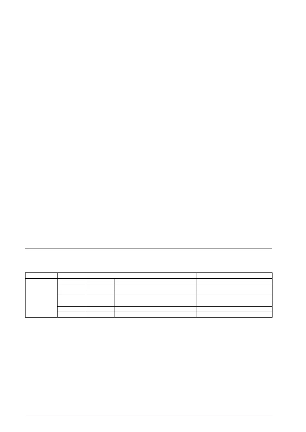
6.1 I/O Map (S1C17 Core I/O Area)Table 3.
Peripheral Address Register name Function
S1C17 Core I/O 0xffff84 IDIR Processor ID Register Indicates the processor ID.
0xffff90 DBRAM Debug RAM Base Register Indicates the debug RAM base address.
0xffffa0 DCR Debug Control Register Debug control
0xffffb4 IBAR1 Instruction Break Address Register 1 Instruction break address #1 setting
0xffffb8 IBAR2 Instruction Break Address Register 2 Instruction break address #2 settin
g
0xffffbc IBAR3 Instruction Break Address Register 3 Instruction break address #3 setting
0xffffd0 IBAR4 Instruction Break Address Register 4 Instruction break address #4 setting
See “Processor Information” in the “CPU” chapter for more information on IDIR. See the “On-chip Debugger
(DBG)” chapter for more information on other registers.
This area includes the S1C17 Core registers, in addition to those des
cribed above. For more information on these
registers, refer to the “S1C17 Core Manual.”



 To Next Page