7 CLOCK GENERATOR (CLG)
7-14
Seiko Epson Corporation
S1C17624/604/622/602/621 TECHNICAL MANUAL
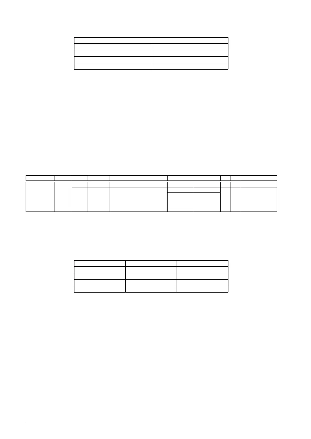
9.5 FOUTH clock (HSCLK Division Ratio) SelectionTable 7.
FOUTHD[1:0] Division ratio
0x3 Reserved
0x2 1/4
0x1 1/2
0x0 1/1
(Default: 0x0)
D1 FOUTHE: FOUTH Output Enable Bit
Enables or disables FOUTH clock (divided HSCLK clock) external output.
1 (R/W): Enabled (on)
0 (R/W): Disabled (off) (default)
Setting FOUTHE to 1 outputs the FOUTH clock from the FOUTH pin. Setting it to 0 stops the output.
D0 FOUT1E: FOUT1 Output Enable Bit
Enables or disables FOUT1 clock (OSC1 clock) external output.
1 (R/W): Enabled (on)
0 (R/W): Disabled (o
ff) (default)
Setting FOUT1E to 1 outputs the FOUT1 clock from the FOUT1 pin. Setting it to 0 stops the output.
PCLK Control Register (CLG_PCLK)
Register name Address Bit Name Function Setting Init. R/W Remarks
PCLK Control
Register
(CLG_PCLK
)
0x5080
(8 bits)
D7–2
–
reserved – – – 0 when being read.
D1–0
PCKEN[1:0]
PCLK enable PCKEN[1:0] PCLK supply 0x3 R/W
0x3
0x2
0x1
0x0
Enable
Not allowed
Not allowed
Disable
D[7:2] Reserved
D[1:0] PCKEN[1:0]: PCLK Enable Bits
Enables or disables clock (PCLK) supply to the internal peripheral modules.
Also set PRUN/PSC_CTL register.
9.6 PCLK ControlTable 7.
PCKEN[1:0] PRUN PCLK supply
0x3 1 Enabled (on)
0x2 * Setting prohibited
0x1 * Setting prohibited
0x0 0 Disabled (off)
(Default: PCKEN[1:0] = 0x3, PRUN = 0)
Peripheral modules that use PCLK
• 16-bit timer (T16)
• 8-bit timer (T8F)
• UART
• SPI
• I
2
C master (I2CM)
• I
2
C slave (I2CS)
• 16-bit PWM timer (T16E)
• I/O port (P)
• MISC register (MISC)
• Power generator (VD1)
• Supply voltage detector (SVD)
•
IR remote controller (REMC)
• A/D converter (ADC10)
• Interrupt controller (ITC)
 Loading...