1 OVERVIEW
S1C17624/604/622/602/621 TECHNICAL MANUAL
Seiko Epson Corporation
1-13
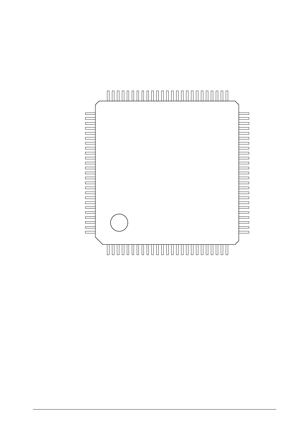
S1C17602/621 Pin Configuration Diagram1.3.4
TQFP14-100pin (S1C17602/621)
1
2
3
4
5
6
7
8
9
10
11
12
13
14
15
16
17
18
19
20
21
22
23
24
25
75
74
73
72
71
70
69
68
67
66
65
64
63
62
61
60
59
58
57
56
55
54
53
52
51
SEG1
SEG2
SEG3
SEG4
SEG5
SEG6
SEG7
SEG8
SEG9
SEG10
SEG11
SEG12
SEG13
SEG14
SEG15
SEG16
SEG17
SEG18
SEG19
SEG20
SEG21
SEG22
SEG23
SEG24
SEG25
AV
DD
V
SS
P15(EXCL3)/AIN5
P14(EXCL2)/AIN6
P13(EXCL1)/AIN7
P12/SIN0
P11/SOUT0
P10/SCLK0
P07/#SPISS0
P06/SDI0
P05/SDO0
P04/SPICLK0
P03/#ADTRG
P02(EXCL0)
P01/REMI
P00/REMO
#RESET
#TEST
OSC1
OSC2
V
D1
V
SS
OSC3
OSC4
V
DD
50
49
48
47
46
45
44
43
42
41
40
39
38
37
36
35
34
33
32
31
30
29
28
27
26
76
77
78
79
80
81
82
83
84
85
86
87
88
89
90
91
92
93
94
95
96
97
98
99
100
V
SS
VC1
V
C2
VC3
CA
CB
N.C.
COM0
COM1
COM2
COM3
SEG39/COM4
SEG38/COM5
SEG37/COM6
SEG36/COM7
SEG35
SEG34
SEG33
SEG32
SEG31
SEG30
SEG29
SEG28
SEG27
SEG26
SCLK1/AIN4/P16
AIN3/P17
AIN2/P20
AIN1/P21
AIN0/P22
V
DD
SENB0/P23
SENA0/P24
REF0/P25
RFIN0/P26
V
SS
SOUT1/RFIN1/P27
SIN1/REF1/P30
SCL0/SENA1/P31
SDA0/SENB1/P32
SCL1/SCL0/P33
SDA1/SDA0/P34
FOUT1/#BFR/P35
TOUT3/RFCLKO/P36
TOUTN3/LFRO/TOUT4/P37
FOUTH/P40
P41/DSIO
P42/DST2
P43/DCLK
SEG0
S1C17602/621
3.4.1 S1C17602/621 Pin Configuration Diagram (TQFP14-100pin)Figure 1.
* The S1C17602/621 (TQFP14-100pin) has the same pin configuration as that of the S1C17604 (TQFP14-100pin).
However, 16-bit PWM timer (T16A2) input/output signals (EXCL5, TOUTA5/CAPA5, TOUTB5/CAPB5,
EXCL6, TOUTA6/CAPA6, and TOUTB6/CAPB6) are not assigned to the S1C17602/621 pins.



 To Next Page