3 MEMORY MAP
S1C17624/604/622/602/621 TECHNICAL MANUAL
Seiko Epson Corporation
3-3
Bus Cycle3.1
The CPU operates with CCLK as the operating clock. For CCLK, see “Controlling the CPU Core Clock (CCLK)”
in the “Clock Generator (CLG)” chapter.
The period between a CCLK rising edge and the next rising edge is assumed to be one CCLK (= one bus cycle). As
shown in Figures 3.1 to 3.3, the number of cycles required for one bus access depends on the peripheral or memory
module. Furthermo
re, the number of bus accesses depends on the CPU instruction (access size) and device size.
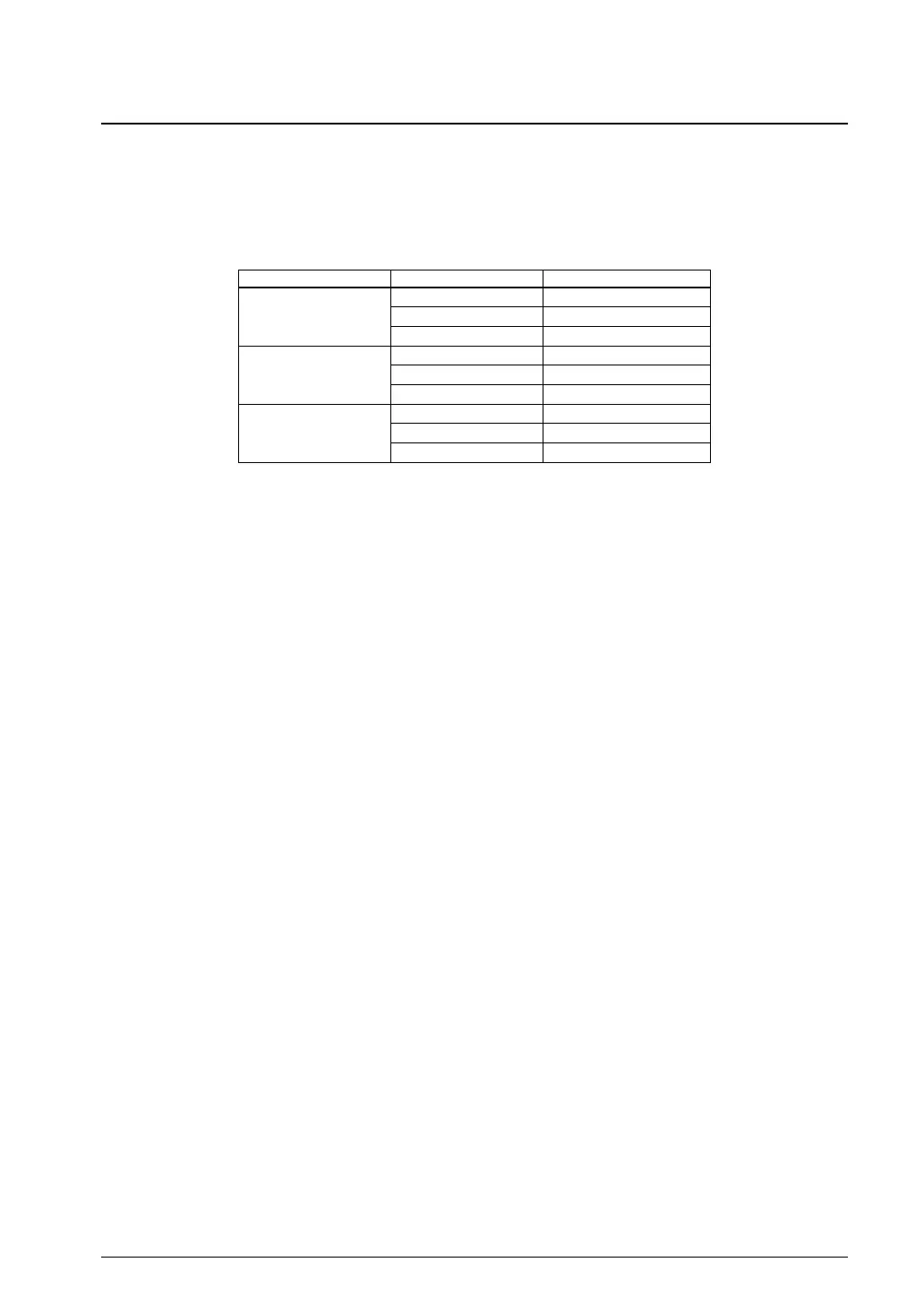
1.1 Number of Bus AccessesTable 3.
Device size CPU access size Number of bus accesses
8 bits 8 bits 1
16 bits 2
32 bits* 4
16 bits 8 bits 1
16 bits 1
32 bits* 2
32 bits 8 bits 1
16 bits 1
32 bits* 1
* Handling the eight high-order bits during 32-bit accesses
During writing, the eight high-order bits are written as 0. During reading from a memory, the eight high-order
bits are ignored. However, the stack operation in an interrupt handling reads/write
s 32-bit data that consists of the
PSR value as the high-order 8 bits and the return address as the low order 24 bits.
Number of bus cycles calculation example
Number of bus cycles when the CPU accesses the display RAM area (eight-bit device, set to two access cycles)
by a 16-bit read or write instruction.
2 [cycles] × 2 [bus accesses] = 4 [CCLK cycles]
Restrictions on Access Size3.1.1
The modules shown below have a restriction on the access size. Appropriate instructions should be used in pro-
gramming.
Flash memory
The Flash memory allows only 16-bit write instructions for programming. Reading data from the Flash memory
has no such restriction.
Other modules can be accessed with an 8-bit, 16-bit, or 32-bit instruction. However, reading for an unnecessary
register may change the peripheral
module status and it may cause a problem. Therefore, use the appropriate in-
structions according to the device size.
Restrictions on Instruction Execution Cycles3.1.2
An instruction fetch and a data access are not performed simultaneously under one of the conditions listed below.
This prolongs the instruction fetch cycle for the number of data area access cycles.
• When the CPU executes the instruc
tion stored in the Flash area and accesses data in the Flash area or display
RAM area
• When the CPU executes the instruction stored in the internal RAM area and accesses data in the internal RAM
area