7 CLOCK GENERATOR (CLG)
S1C17624/604/622/602/621 TECHNICAL MANUAL
Seiko Epson Corporation
7-9
Clock External Output (FOUTH, FOUT1)7.7
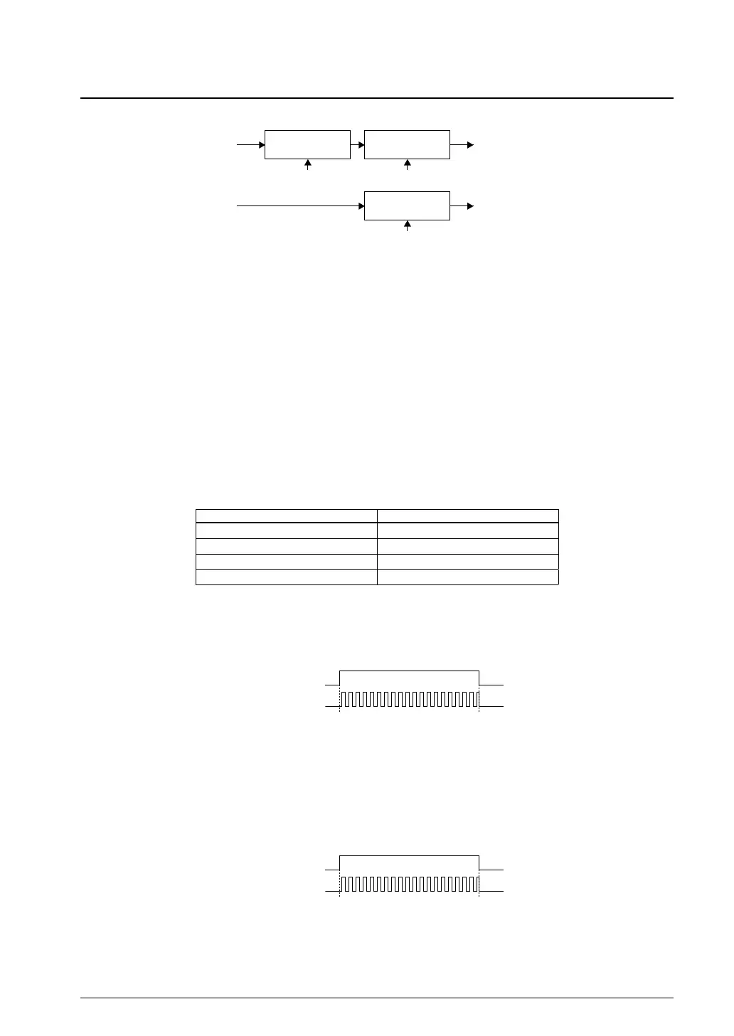
A divided HSCLK (IOSC/OSC3) clock or the OSC1 clock can be output to external devices.
Divider
(1/1–1/4)
HSCLK clock
FOUTH
output circuit
On/Off controlDivision ratio selection
OSC1 clock
FOUT1
output circuit
On/Off control
I/O port (FOUTH pin)
I/O port (FOUT1 pin)
7.1 Clock Output CircuitFigure 7.
There are two output systems available: FOUTH and FOUT1.
Output pin setting
The FOUTH and FOUT1 output pins are shared with I/O ports. The pin is configured for the I/O port by de-
fault, so the pin function should be changed using the port function select bit before the clock output can be
used. See the “I/O Ports (P)” chapter for the FOUTH/FOUT1 pins and selectin
g pin functions.
FOUTH output control
FOUTH is a divided HSCLK (IOSC or OSC3) clock.
FOUTH clock frequency selection
Three different clock output frequencies can be selected. Select the division ratio for the HSCLK clock us-
ing FOUTHD[1:0]/OSC_FOUT register.
7.1 FOUTH clock (HSCLK Division Ratio) SelectionTable 7.
FOUTHD[1:0] Division ratio
0x3 Reserved
0x2 1/4
0x1 1/2
0x0 1/1
(Default: 0x0)
Clock output control
The clock output is controlled using FOUTHE/OSC_FOUT register. Setting FOUTHE to 1 outputs the
FOUTH clock from the FOUTH pin. Setting it to 0 disables output.
7.2 FOUTH OutputFigure 7.
FOUT1 output
FOUT1 is the OSC1 clock.
Clock output control
The clock output is controlled using FOUT1E/OSC_FOUT register. Setting FOUT1E to 1 outputs the
FOUT1 clock from the FOUT1 pin. Setting it to 0 disables output.
7.3 FOUT1 OutputFigure 7.
Note: Since the FOUTH/FOUT1 signal is not synchronized with FOUTHE/FOUT1E writing, switching
output on or off will generate certain hazards.



 To Next Page