9 I/O PORTS (P)
S1C17624/604/622/602/621 TECHNICAL MANUAL
Seiko Epson Corporation
9-9
D[7:0] PxPU[7:0]: Px[7:0] Port Pull-up Enable Bits
Enables or disables the pull-up resistor included in each port.
1 (R/W): Enabled (default)
0 (R/W): Disabled
PxPUy is the pull-up control bit that corresponds directly to the Pxy port. Setting to 1 enables the pull-
up resistor and the port pin will be pulled up when output is disabled (PxOENy = 0). When PxPUy is set
to 0, the pin will not be pulled up.
When output is enabled (PxOENy = 1), the
PxPUy setting is ignored, and the pin is not pulled up.
I/O ports that are not used should be set with pull-up enabled.
This pull-up setting is also enabled for ports for which the peripheral module input function is selected.
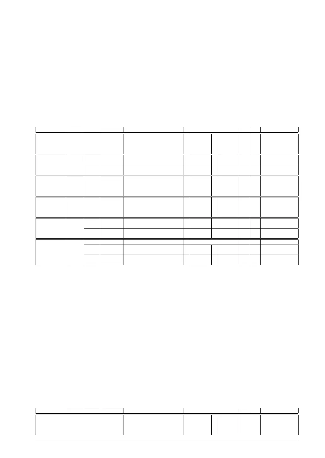
Px Port Schmitt Trigger Control Registers (Px_SM)
Register name Address Bit Name Function Setting Init. R/W Remarks
P0 Port Schmitt
Trigger Control
Register
(P0_SM)
0x5204
(8 bits)
D7–0
P0SM[7:0]
P0[7:0] port Schmitt trigger input
enable
1 Enable
(Schmitt)
0 Disable
(CMOS)
1 R/W
P1 Port Schmitt
Trigger Control
Register
(P1_SM)
0x5214
(8 bits)
D7–6
P1SM[7:6]
P1[7:6] port Schmitt trigger input
enable
1 Enable
(Schmitt)
0 – 1 R Always enabled
D5–0
P1SM[5:0]
P1[5:0] port Schmitt trigger input
enable
1 Enable
(Schmitt)
0 Disable
(CMOS)
1 R/W
P2 Port Schmitt
Trigger Control
Register
(P2_SM)
0x5224
(8 bits)
D7–0
P2SM[7:0]
P2[7:0] port Schmitt trigger input
enable
1 Enable
(Schmitt)
0 – 1 R Always enabled
P3 Port Schmitt
Trigger Control
Register
(P3_SM)
0x5234
(8 bits)
D7–0
P3SM[7:0]
P3[7:0] port Schmitt trigger input
enable
1 Enable
(Schmitt)
0 – 1 R Always enabled
P4 Port Schmitt
Trigger Control
Register
(P4_SM)
0x5244
(8 bits)
D7–4
P4SM[7:4]
P4[7:4] port Schmitt trigger input
enable
1 Enable
(Schmitt)
0 Disable
(CMOS)
1 R/W D[7:4] = reserved in
S1C17604/602/621
D3–0
P4SM[3:0]
P4[3:0] port Schmitt trigger input
enable
1 Enable
(Schmitt)
0 – 1 R Always enabled
P5 Port Schmitt
Trigger Control
Register
(P5_SM)
(S1C17624/622)
0x5254
(8 bits)
D7
–
reserved – – – 0 when being read.
D6–3
P5SM[6:3]
P5[6:3] port Schmitt trigger input
enable
1 Enable
(Schmitt)
0 – 1 R Always enabled
D2–0
P5SM[2:0]
P5[2:0] port Schmitt trigger input
enable
1 Enable
(Schmitt)
0 Disable
(CMOS)
1 R/W
Note: The PxSMy bits for unavailable ports are reserved and always read as 0.
D[7:0] PxSM[7:0]: Px[7:0] Port Schmitt Trigger Input Enable Bits
Enables or disables the Schmitt trigger input buffer for each port.
1 (R/W): Enable (Schmitt) (default)
0 (R/W): D
isable (CMOS level)
PxSMy is the Schmitt input control bit that corresponds directly to the Pxy port. Setting to 1 enables the
Schmitt input buffer, and setting to 0 uses the CMOS level input buffer.
The I/O ports shown below support only CMOS Schmitt input.
S1C17624/622: P1[7:6], P2[7:0], P3[7:0], P40, DSIO/P41, DST2/P42, DCLK/P43*, P5[6:3]
S1C17604/602/621: P1[7:6], P2[7:0], P3[7:0], P40, DSIO/P4
1, DST2/P42, DCLK/P43*
(* P43 is an output-only port.)
In the
S1C17624/622/604, the
PxSMy
bits for these ports are read-only bits that are always read as 1. In
the S1C17602/621, both 1 and 0 can be written to and read from these bits. However, the input interface
level cannot be switched.
Px Port Interrupt Mask Registers (Px_IMSK)
Register name Address Bit Name Function Setting Init. R/W Remarks
Px Port
Interrupt Mask
Register
(Px_IMSK)
0x5205
0x5215
(8 bits)
D7–0
PxIE[7:0]
Px[7:0] port interrupt enable 1 Enable 0 Disable 0 R/W



 To Next Page