24 A/D CONVERTER (ADC10)
S1C17624/604/622/602/621 TECHNICAL MANUAL
Seiko Epson Corporation
24-1
A/D Converter (ADC10)24
ADC10 Module Overview24.1
The S1C17624/604/622/602/621 includes an A/D converter (ADC10) that converts analog input signals into 10-bit
digital values.
The following shows the features of the ADC10 module:
• Conversion method: Successive approximation type
• Resolution: 10 bits
• Input channels: Max. 8 channels
• A/D conversion clock: Max. 2 MHz
• Sampling rate: f
ADCLK/13 to fADCLK/20 [sps] (fADCLK: A/D conversion clock frequency)
• Analog input voltage range: V
SS to AVDD (= VDD)
• Sampling & hold circuit included
• Supports two conversion modes: One-time conversion mode
(for single channel or multi-channels)
Continuous conversion mode
(for single channel or multi-channels, terminated with software)
• Supports three conversion triggers: Software trigger
Exte
rnal trigger (input from the #ADTRG pin)
T16 Ch.0 underflow trigger
• The conversion results can be read as 16-bit data with the 10-bit converted data aligned to left or right.
• Two types of interrupts can be generated: Conversion completion interrupt
Conversion data overwrite error interrupt
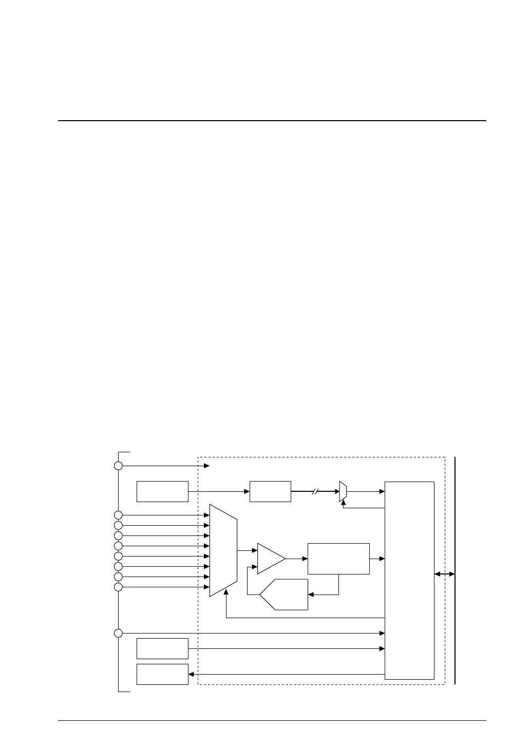
Figure 24.1.1 shows the ADC10 configuration.
Bus I/F
and
control
registers
Interrupt request
Trigger signals
ADC10
External trigger
Successive
approximation
control circuit
D/A
converter
Internal data bus
AVDD
#ADTRG
Multi-
plexer
AIN7
AIN6
AIN5
AIN4
AIN3
AIN2
AIN1
AIN0
+
–
PCLK
CLG
Divider
(1/2–1/32K)
T16 Ch.0
ITC
ADCLK
1.1 A/D Converter ConfigurationFigure 24.



 To Next Page