23 LCD DRIVER (LCD)
23-18
Seiko Epson Corporation
S1C17624/604/622/602/621 TECHNICAL MANUAL
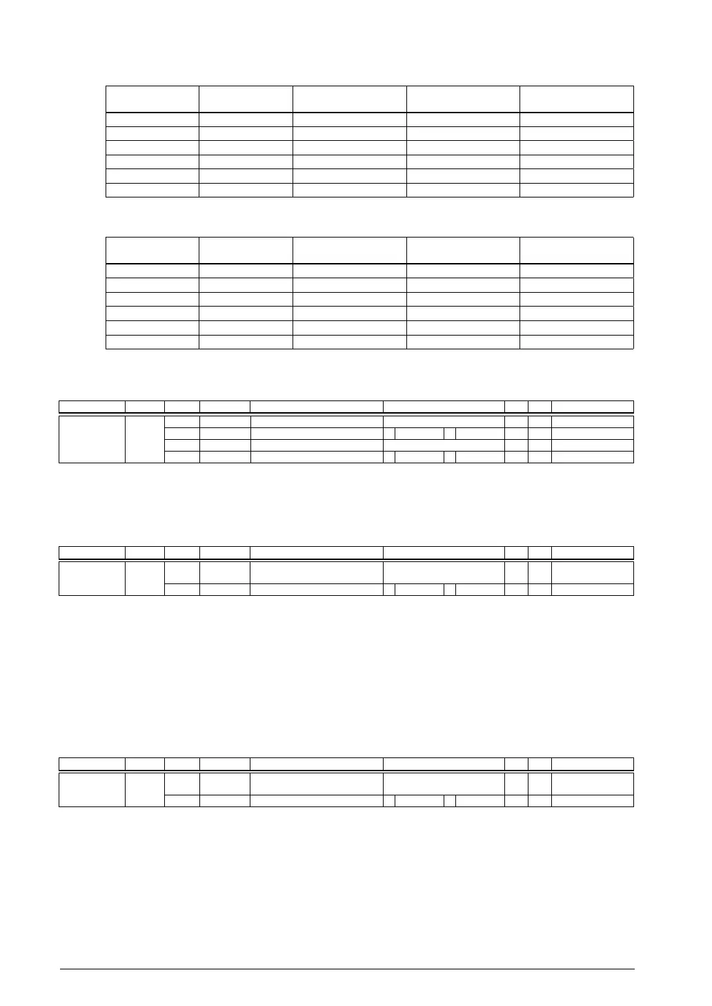
8.7 Drive Duty Settings (S1C17624/622)Table 23.
LDUTY[2:0] Duty Valid COM pins Valid SEG pins
Max. number of
display segments
0x7–0x5 Reserved – – –
0x4 1/8 COM0 to COM7 SEG0 to SEG51 416 segments
0x3 1/4 COM0 to COM3 SEG0 to SEG55 224 segments
0x2 1/3 COM0 to COM2 SEG0 to SEG55 168 segments
0x1 1/2 COM0 to COM1 SEG0 to SEG55 112 segments
0x0 Static COM0 SEG0 to SEG55 56 segments
(Default: 0x4)
8.8 Drive Duty Settings (S1C17604/602/621)Table 23.
LDUTY[2:0] Duty Valid COM pins Valid SEG pins
Max. number of
display segments
0x7–0x5 Reserved – – –
0x4 1/8 COM0 to COM7 SEG0 to SEG35 288 segments
0x3 1/4 COM0 to COM3 SEG0 to SEG39 160 segments
0x2 1/3 COM0 to COM2 SEG0 to SEG39 120 segments
0x1 1/2 COM0 to COM1 SEG0 to SEG39 80 segments
0x0 Static COM0 SEG0 to SEG39 40 segments
(Default: 0x4)
LCD Voltage Regulator Control Register (LCD_VREG)
Register name Address Bit Name Function Setting Init. R/W Remarks
LCD Voltage
Regulator
Control Register
(LCD_VREG)
0x50a3
(8 bits)
D7–5
–
reserved – – – 0 when being read.
D4
LHVLD
LCD heavy load protection mode
1 On 0 Off 0 R/W
D3–1
–
reserved – – – 0 when being read.
D0
VCSEL
V
C reference voltage select 1 VC2 0 VC1 0 R/W
For more information on the control bit, see “LCD Voltage Regulator Control Register (LCD_VREG)” in the “Power
Supply” chapter.
LCD Interrupt Mask Register (LCD_IMSK)
Register name Address Bit Name Function Setting Init. R/W Remarks
LCD Interrupt
Mask Register
(LCD_IMSK)
0x50a5
(8 bits)
D7–1
–
reserved – – – 0 when being read.
D0
FRMIE
Frame signal interrupt enable 1 Enable 0 Disable 0 R/W
D[7:1] Reserved
D0 FRMIE: Frame Signal Interrupt Enable Bit
Enables or disables frame interrupts.
1 (R/W): Interrupt enabled
0 (R/W): Interrupt disabled (default)
Setting FRMIE to 1 enables LCD interrupt requests to the ITC. Setting to 0 disables interrupts.
LCD Interrupt Flag Register (LCD_IFLG)
Register name Address Bit Name Function Setting Init. R/W Remarks
LCD Interrupt
Flag Register
(LCD_IFLG)
0x50a6
(8 bits)
D7–1
–
reserved – – – 0 when being read.
D0
FRMIF
Frame signal interrupt flag 1 Occurred 0
Not occurred
0 R/W Reset by writing 1.
D[7:1] Reserved
D0 FRMIF: Frame Signal Interrupt Flag Bit
Indicates the frame interrupt cause occurrence status.
1 (R): Cause of interrupt has occurred
0 (R): No cause of interrupt has occurred (default)
1 (W): Flag is reset
0 (W): Ignored
FRMIF is set to 1 at the frame signal rising edge. FRMIF is reset to 0 by writing 1.