4 POWER SUPPLY
4-4
Seiko Epson Corporation
S1C17624/604/622/602/621 TECHNICAL MANUAL
D5 HVLD: VD1 Heavy Load Protection Mode Bit
Sets the internal logic voltage regulator into heavy load protection mode.
1 (R/W): Heavy load protection On
0 (R/W): Heavy load protection Off (default)
The internal logic voltage regulator enters heavy load protection mode by writing 1 to HVLD and it
ensures stable V
D1 output. Use the heavy load protection function when a heavy load such as a lamp or
buzzer is driven with a port output (
see Section 4.5). Current consumption increases in heavy load pro-
tection mode, therefore do not set if unnecessary.
D[4:1] Reserved
D0 VD1MD: Flash Erase/Programming Mode Bit
Selects the V
D1 internal operating voltage value (operating mode).
1 (R/W): V
D1 = 2.5 V, Flash erase/programming mode
0 (R/W): V
D1 = 1.8 V, Normal operating mode (default)
Normally set VD1MD to 0 (V
D1 = 1.8 V, default setting). It should be set to 1 before erasing/program-
ming t
he Flash memory.
Note: When the V
D1 voltage is switched, the VD1 voltage requires 5 ms (max.) to stabilize. Flash memory
programming should be started after the stabilization time has elapsed.
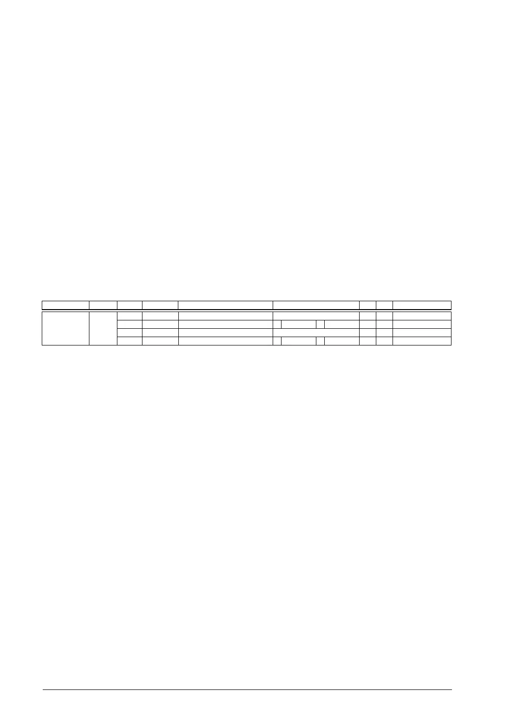
LCD Voltage Regulator Control Register (LCD_VREG)
Register name Address Bit Name Function Setting Init. R/W Remarks
LCD Voltage
Regulator
Control Register
(LCD_VREG)
0x50a3
(8 bits)
D7–5
–
reserved – – – 0 when being read.
D4
LHVLD
LCD heavy load protection mode
1 On 0 Off 0 R/W
D3–1
–
reserved – – – 0 when being read.
D0
VCSEL
V
C reference voltage select 1 VC2 0 VC1 0 R/W
D[7:5] Reserved
D4 LHVLD: LCD Heavy Load Protection Mode Bit
Sets the LCD system voltage regulator into heavy load protection mode.
1 (R/W): Heavy load protection On
0 (R/W): Heavy load protection Off (default)
The LCD system voltage regulator enters heavy load protection mode by writing 1
to LHVLD and it
ensures stable V
C1–VC3 outputs. Use the heavy load protection function when the LCD display has in-
consistencies in density. Current consumption increases in heavy load protection mode, therefore do not
set if unnecessary.
D[3:1] Reserved
D0 VCSEL: V
C Reference Voltage Select Bit
Selects the reference voltage for the LCD voltage booster/reducer according to the power supply
voltage V
DD.
1 (R/W): V
C2 is used as the reference voltage
0
(R/W): VC1 is used as the reference voltage (default)
As compared to the V
C1 reference voltage, the VC2 reference voltage is lower in current consumption.
Set VCSEL to 0 when V
DD is less than 2.5 V.
Note: The V
C1 to VC3 voltages cannot be obtained correctly if VCSEL is set to 1 when VDD is less
than 2.5 V.



 To Next Page