29 ELECTRICAL CHARACTERISTICS
S1C17624/604/622/602/621 TECHNICAL MANUAL
Seiko Epson Corporation
29-9
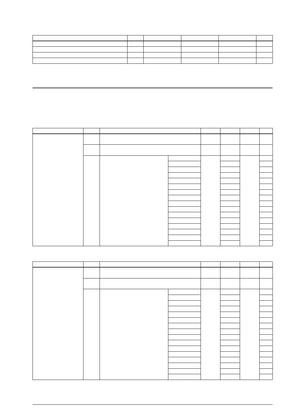
Unless otherwise specified: VDD = 1.8 to 3.6V, VSS = 0V, Ta = -25 to 70°C
Item Symbol Min. Typ. Max. Unit
SCL cycle time t
SCL 2500 ns
Start condition hold time t
STH 1/fSYS ns
Data output delay time t
SDD 1/fSYS ns
Stop condition hold time t
SPH 1/fSYS ns
* f
SYS: System operating clock frequency
LCD Driver Characteristics29.9
The typical values in the following LCD driver characteristics varies depending on the panel load (panel size, drive
duty, number of display pixels and display contents),
so evaluate them by connecting to the actually used LCD panel.
LCD drive voltage
Unless otherwise specified: VDD = 2.5 to 3.6V, VSS = 0V, Ta = 25°C, C2–C5 = 0.1µF, Checker pattern displayed, No panel load,
VCSEL = 1 (V
C2 reference voltage)
Item Symbol Condition Min. Typ. Max. Unit
LCD drive voltage
(V
C2 reference voltage)
V
C1 Connect 1MW load resistor between VSS and VC1 0.324 ×
V
C3(Typ.)
0.350 ×
VC3(Typ.)
V
V
C2 Connect 1MW load resistor between VSS and VC2 0.649 ×
V
C3(Typ.)
0.701 ×
VC3(Typ.)
V
V
C3 Connect 1MW load resistor
between V
SS and VC3
LC[3:0] = 0x0
Typ. ×
0.96
2.56
Typ. ×
1.04
V
LC[3:0] = 0x1 2.62 V
LC[3:0] = 0x2 2.68 V
LC[3:0] = 0x3 2.74 V
LC[3:0] = 0x4 2.80
V
LC[3:0] = 0x5 2.86 V
LC[3:0] = 0x6 2.92 V
LC[3:0] = 0x7 2.98 V
LC[3:0] = 0x8 3.04 V
LC[3:0] = 0x9 3.10 V
LC[3:0] = 0xa 3.15 V
LC[3:0] = 0xb 3.21 V
LC[3:0] = 0xc 3.27 V
LC[3:0] = 0xd 3.33 V
LC[3:0] = 0xe 3.39 V
LC[3:0] = 0xf 3.45 V
Unless otherwise specified: V
DD = 1.8 to 3.6V, VSS = 0V, Ta = 25°C, C2–C5 = 0.1µF, Checker pattern displayed, No panel load,
VCSEL = 0 (V
C1 reference voltage)
Item Symbol Condition Min. Typ. Max. Unit
LCD drive voltage
(V
C1 reference voltage)
V
C1 Connect 1MW load resistor between VSS and VC1 0.333 ×
V
C3(Typ.)
0.360 ×
VC3(Typ.)
V
V
C2 Connect 1MW load resistor between VSS and VC2 0.645 ×
V
C3(Typ.)
0.696 ×
VC3(Typ.)
V
V
C3 Connect 1MW load resistor
between V
SS and VC3
LC[3:0] = 0x0
Typ. ×
0.96
2.50
Typ. ×
1.04
V
LC[3:0] = 0x1 2.56 V
LC[3:0] = 0x2 2.61 V
LC[3:0] = 0x3 2.67 V
LC[3:0] = 0x4 2.73
V
LC[3:0] = 0x5 2.79 V
LC[3:0] = 0x6 2.85 V
LC[3:0] = 0x7 2.90 V
LC[3:0] = 0x8 2.96 V
LC[3:0] = 0x9 3.02 V
LC[3:0] = 0xa 3.08 V
LC[3:0] = 0xb 3.14 V
LC[3:0] = 0xc 3.19 V
LC[3:0] = 0xd 3.25 V
LC[3:0] = 0xe 3.31 V
LC[3:0] = 0xf 3.37 V



 To Next Page