9 I/O PORTS (P)
S1C17624/604/622/602/621 TECHNICAL MANUAL
Seiko Epson Corporation
9-1
I/O Ports (P)9
P Module Overview9.1
The P ports are general-purpose digital inputs/outputs that allow software to control the input/output direction, pull-
up resistor, and input interface level. These ports are shared with internal peripheral module inputs/outputs, and the
pin functions can be switched by setting the registers. A number of port groups can generate interrupts caused by a
transiti
on of the input signal.
The following shows the features of the P module:
• S1C17624/622: Maximum 47 I/O ports (P0[7:0], P1[7:0], P2[7:0], P3[7:0], P4[7:0], P5[6:0]) are available.
S1C17604/602/621: Maximum 36 I/O ports (P0[7:0], P1[7:0], P2[7:0], P3[7:0], P4[3:0]) are available.
* The number of ports for general-purpose use depends on the peripheral functions used.
• Each port has a pull-up resistor
that can be enabled with software.
• Some I/O ports support two input interface levels selectable with software: CMOS Schmitt level or CMOS level
• The P0 and P1 ports can generate input interrupts at the signal edge selected with software.
• The P0 and P1 ports include a chattering filter.
• Can generate an initial reset by entering low level simultaneously to the P0 ports selected with software.
• Al
l port provide a port function select bit to configure the pin function (for GPIO or peripheral functions).
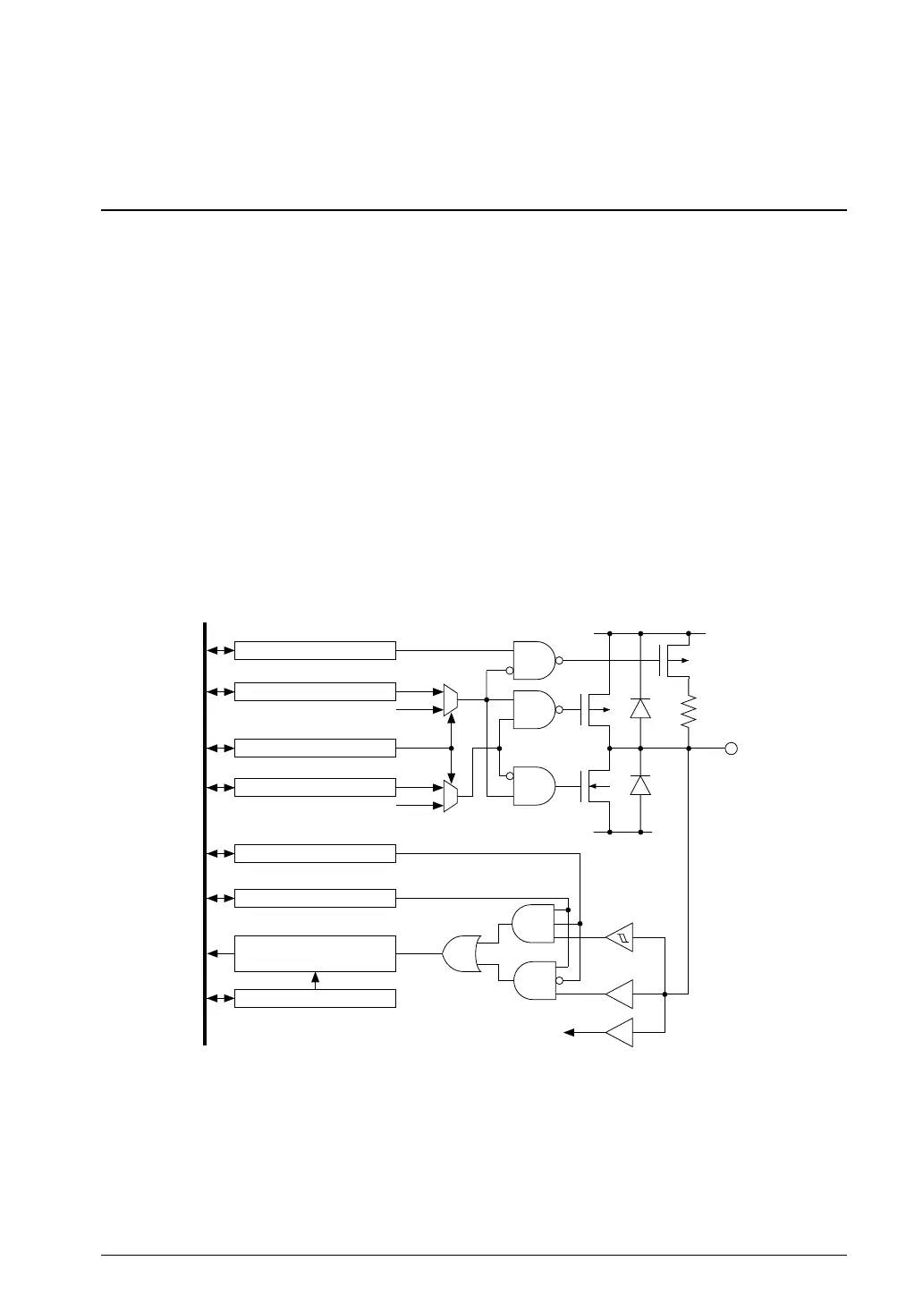
Figure 9.1.1 shows the I/O port configuration.
Peripheral output
Peripheral I/O control
PxPUy
PxOENy
PxSMy
PxOUTy
PxyMUX
Pull-up enable
Output enable
Schmitt trigger control
Output data
Function selection
V
DD
VSS
Internal data bus
Pxy
Peripheral module input
PxIENy
PxCF1[2:0]/PxCF2[2:0]
Chattering filter
(P0, P1)
Input enable
1.1 I/O Port ConfigurationFigure 9.
Notes: • The PCLK clock must be supplied from the clock generator to access the I/O port. The PCLK
clock is also needed to operate the P0/P1 chattering filters.
• The “xy” in the register and bit names refers to the port number (Pxy, x = 0 to 5, y = 0 to 7).
Example: PxINy/Px_IN register
P00: P0IN0/P0_IN register
P17: P1IN7/P1_IN register
 Loading...