9 I/O PORTS (P)
S1C17624/604/622/602/621 TECHNICAL MANUAL
Seiko Epson Corporation
9-7
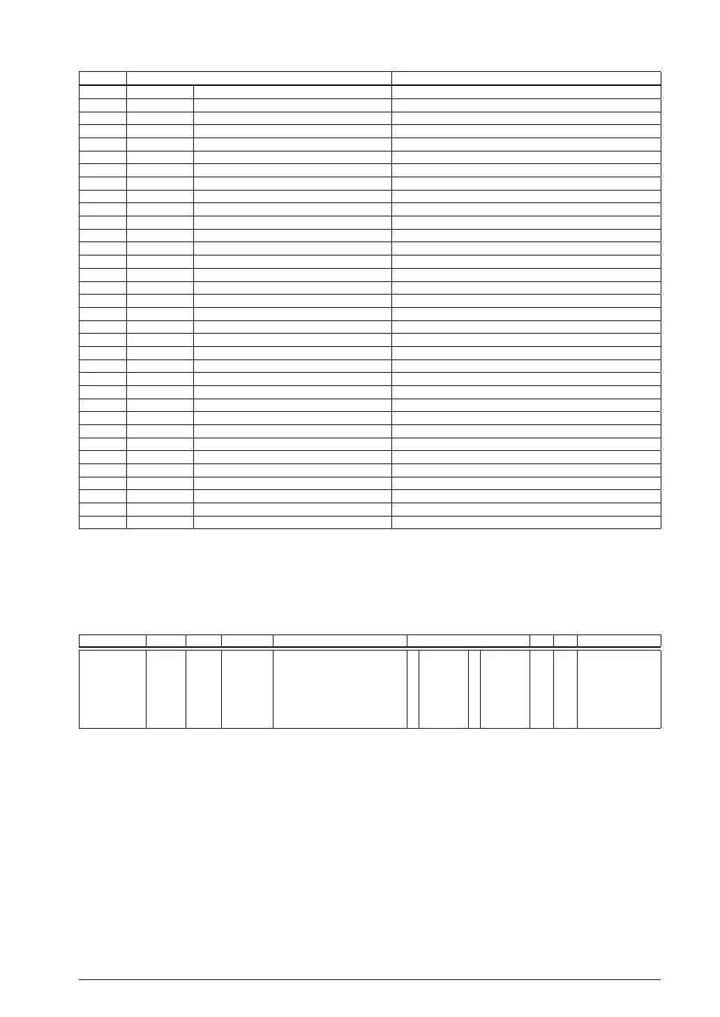
Address Register name Function
0x5222 P2_OEN P2 Output Enable Register Enables P2 port outputs.
0x5223 P2_PU P2 Port Pull-up Control Register Controls the P2 port pull-up resistor.
0x5224 P2_SM P2 Port Schmitt Trigger Control Register Controls the P2 port Schmitt trigger input.
0x522a P2_IEN
P2 Port Input Enable Register
Enables P2 port inputs.
0x5230 P3_IN P3 Port Input Data Register P3 port input data
0x5231 P3_OUT P3 P
ort Output Data Register P3 port output data
0x5232 P3_OEN P3 Port Output Enable Register Enables P3 port outputs.
0x5233 P3_PU P3 Port Pull-up Control Register Controls the P3 port pull-up resistor.
0x5234 P3_SM P3 Port Schmitt Trigger Control Register Controls the P3 port Schmitt trigger input.
0x523a P3_IEN
P3 Port Input Enable Register
Enables P3 port inputs.
0x5240 P4_IN P4 Port Input Data Register P4 port input
data
0x5241 P4_OUT P4 Port Output Data Register P4 port output data
0x5242 P4_OEN P4 Port Output Enable Register Enables P4 port outputs.
0x5243 P4_PU P4 Port Pull-up Control Register Controls the P4 port pull-up resistor.
0x5244 P4_SM P4 Port Schmitt Trigger Control Register Controls the P4 port Schmitt trigger input.
0x524a P4_IEN
P4 Port Input Enable Register
Enables P4 port inputs.
0x5250 P5_IN P5 Port Input Data Re
gister P5 port input data *
0x5251 P5_OUT P5 Port Output Data Register P5 port output data *
0x5252 P5_OEN P5 Port Output Enable Register Enables P5 port outputs. *
0x5253 P5_PU P5 Port Pull-up Control Register Controls the P5 port pull-up resistor. *
0x5254 P5_SM P5 Port Schmitt Trigger Control Register Controls the P5 port Schmitt trigger input. *
0x525a P5_IEN
P5 Port Input Enable Register
Enables P5 port inputs. *
0x52a0 P00_03PMUX P0[3:0] Port Function Select Register Selects the P0[3:0] port functions.
0x52a1 P04_07PMUX P0[7:4] Port Function Select Register Selects the P0[7:4] port functions.
0x52a2 P10_13PMUX P1[3:0] Port Function Select Register Selects the P1[3:0] port functions.
0x52a3 P14_17PMUX P1[7:4] Port Function Select Register Selects the P1[7:4] port functions.
0x52a4 P20_23PMUX P2[3:0] Port Function Select Reg
ister Selects the P2[3:0] port functions.
0x52a5 P24_27PMUX P2[7:4] Port Function Select Register Selects the P2[7:4] port functions.
0x52a6 P30_33PMUX P3[3:0] Port Function Select Register Selects the P3[3:0] port functions.
0x52a7 P34_37PMUX P3[7:4] Port Function Select Register Selects the P3[7:4] port functions.
0x52a8 P40_43PMUX P4[3:0] Port Function Select Register Selects the P4[3:0] port functions.
0x52a9 P4
4_47PMUX P4[7:4] Port Function Select Register Selects the P4[7:4] port functions. *
0x52aa P50_53PMUX P5[3:0] Port Function Select Register Selects the P5[3:0] port functions. *
0x52ab P54_56PMUX P5[6:4] Port Function Select Register Selects the P5[6:4] port functions. *
* Available only for S1C17624/622
The I/O port registers are described in detail below. These are 8-bit registers.
Note: When data is written
to the registers, the “Reserved” bits must always be written as 0 and not 1.
Px Port Input Data Registers (Px_IN)
Register name Address Bit Name Function Setting Init. R/W Remarks
Px Port Input
Data Register
(Px_IN)
0x5200
0x5210
0x5220
0x5230
0x5240
0x5250
(8 bits)
D7–0
PxIN[7:0]
Px[7:0] port input data 1 1 (H) 0 0 (L) × R
Note: The PxINy bits for unavailable ports are reserved and always read as 0.
D[7:0] PxIN[7:0]: Px[7:0] Port Input Data Bits
The port pin status can be read out. (Default: external input status)
1 (R): High level
0 (R): Low level
PxINy corresponds directly to the Pxy pin. The pin voltage level can be read out when input is enabled
(PxIENy = 1) (even if output is also enabled (Px
OENy = 1)). The value read out will be 1 when the pin
voltage is High and 0 when Low.
The value read out is 0 when input is disabled (PxIENy = 0).
Writing operations to the read-only PxINy is disabled.
 Loading...