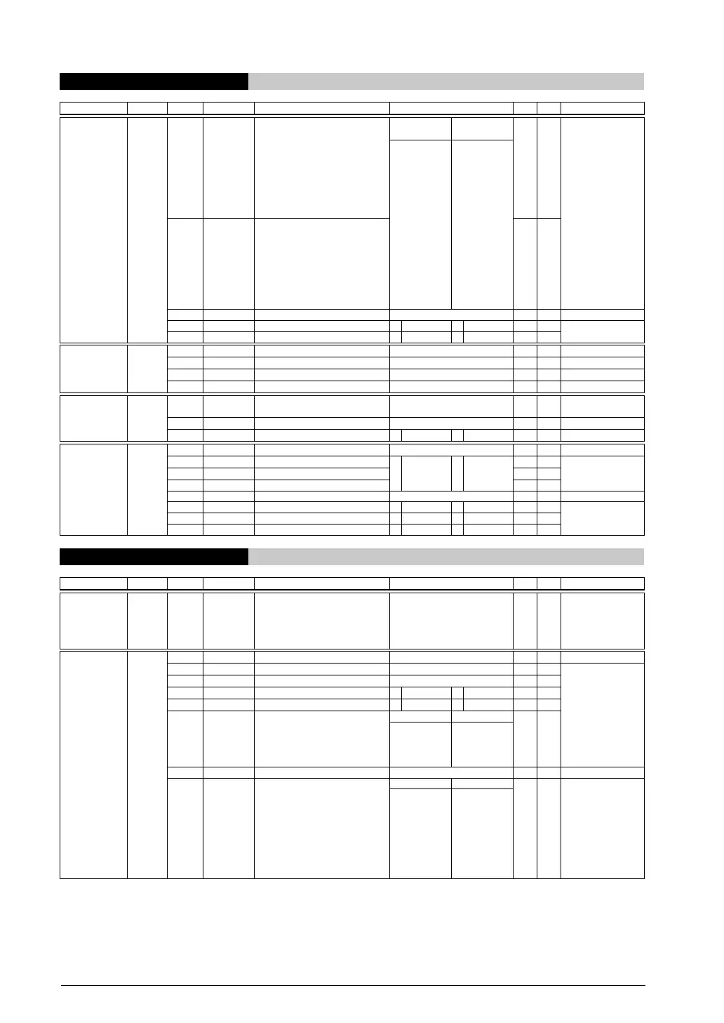
APPENDIX A LIST OF I/O REGISTERS
AP-A-24
Seiko Epson Corporation
S1C17624/604/622/602/621 TECHNICAL MANUAL
0x5340–0x5346 IR Remote Controller
Register name Address Bit Name Function Setting Init. R/W Remarks
REMC
Configuration
Register
(REMC_CFG)
0x5340
(16 bits)
D15–12
CGCLK[3:0]
Carrier generator clock division
ratio select
CGCLK[3:0]
LCCLK[3:0]
Division ratio
0x0 R/W Source clock = PCLK
0xf
0xe
0xd
0xc
0xb
0xa
0x9
0x8
0x7
0x6
0x5
0x4
0x3
0x2
0x1
0x0
reserved
1/16384
1/8192
1/4096
1/2048
1/1024
1/512
1/256
1/128
1/64
1/32
1/16
1/8
1/4
1/2
1/1
D11–8
LCCLK[3:0]
Length counter clock division ratio
select
0x0 R/W
D7–2
–
reserved – – – 0 when being read.
D1
REMMD
REMC mode select
1 Receive 0 Transmit 0 R/W
D0
REMEN
REMC enable
1 Enable 0 Disable 0 R/W
REMC Carrier
Length Setup
Register
(REMC_CAR)
0x5342
(16 bits)
D15–14
–
reserved – – – 0 when being read.
D13–8
REMCL[5:0]
Carrier L length setup 0x0 to 0x3f 0x0 R/W
D7–6
–
reserved – – – 0 when being read.
D5–0
REMCH[5:0]
Carrier H length setup 0x0 to 0x3f 0x0 R/W
REMC Length
Counter Register
(REMC_LCNT)
0x5344
(16 bits)
D15–8
REMLEN[7:0]
Transmit/receive data length count
(down counter)
0x0 to 0xff 0x0 R/W
D7–1
–
reserved – – – 0 when being read.
D0
REMDT
Transmit/receive data
1 1 (H) 0 0 (L) 0 R/W
REMC Interrupt
Control Register
(REMC_INT)
0x5346
(16 bits)
D15–11
–
reserved – – – 0 when being read.
D10
REMFIF
Falling edge interrupt flag 1 Cause of
interrupt
occurred
0 Cause of
interrupt not
occurred
0 R/W Reset by writing 1.
D9
REMRIF
Rising edge interrupt flag 0 R/W
D8
REMUIF
Underflow interrupt flag 0 R/W
D7–3
–
reserved – – – 0 when being read.
D2
REMFIE
Falling edge interrupt enable 1 Enable 0 Disable 0 R/W
D1
REMRIE
Rising edge interrupt enable 1 Enable 0 Disable 0 R/W
D0
REMUIE
Underflow interrupt enable 1 Enable 0 D
isable 0 R/W
0x5380–0x5386 A/D Converter
Register name Address Bit Name Function Setting Init. R/W Remarks
A/D Conversion
Result Register
(ADC10_ADD)
0x5380
(16 bits)
D15–0
ADD[15:0]
A/D converted data
ADD[9:0] are effective when
STMD = 0 (ADD[15:10] = 0)
ADD[15:6] are effective when
STMD = 1 (ADD[5:0] = 0)
0x0 to 0x3ff 0x0 R
A/D Trigger/
Channel Select
Register
(ADC10_TRG
)
0x5382
(16 bits)
D15–14
–
reserved – – – 0 when being read.
D13–11
ADCE[2:0]
End channel select
0x0 to 0x7 0x0 R/W
D10–8
ADCS[2:0]
Start channel select
0x0 to 0x7 0x0 R/W
D7
STMD
Conversion result storing mode 1 ADD[15:6] 0 ADD[9:0] 0 R/W
D6
ADMS
Conversion mode select 1 Continuous 0 Single 0 R/W
D5–4
ADTS[1:0]
Conversion trigger select
ADTS[1:0]
Trigger 0x0 R/W
0x3
0x2
0x1
0x0
#ADTRG pin
reserved
T16 Ch.0
Software
D3
–
reserved – – – 0 when being read.
D2–0
ADST[2:0]
Sampling time setting
ADST[2:0]
Sampling time 0x7 R/W
0x7
0x6
0x5
0x4
0x3
0x2
0x1
0x0
9 cycles
8 cycles
7 cycles
6 cycles
5 cycles
4 cycles
3 cycles
2 cycles



 To Next Page