22 IR REMOTE CONTROLLER (REMC)
22-6
Seiko Epson Corporation
S1C17624/604/622/602/621 TECHNICAL MANUAL
Falling edge interrupt
Generated when the REMI pin input signal changes from High to Low, this interrupt cause sets the interrupt
flag REMFIF/REMC_INT register to 1 within the REMC.
By running the data length counter between this interrupt and a rising edge interrupt when data is being re-
ceived, the received data pulse width can be calculated from that count value.
To use this interrupt, set REMF
IE/REMC_INT register to 1. If REMFIE is set to 0 (default), the interrupt re-
quest attributable to this cause will not be sent to the ITC.
When REMFIF is set to 1, REMC outputs an interrupt request to the ITC. An interrupt will be generated if the
ITC and S1C17 Core interrupt conditions are met.
REMFIF should be inspected in the REMC interrupt handler routine to determine whether the REMC interrup
t
is attributable to input signal falling edge.
The interrupt cause should be cleared in the interrupt handler routine by resetting (writing 1 to) REMFIF.
For more information on interrupt processing, see the “Interrupt Controller (ITC)” chapter.
Control Register Details22.7
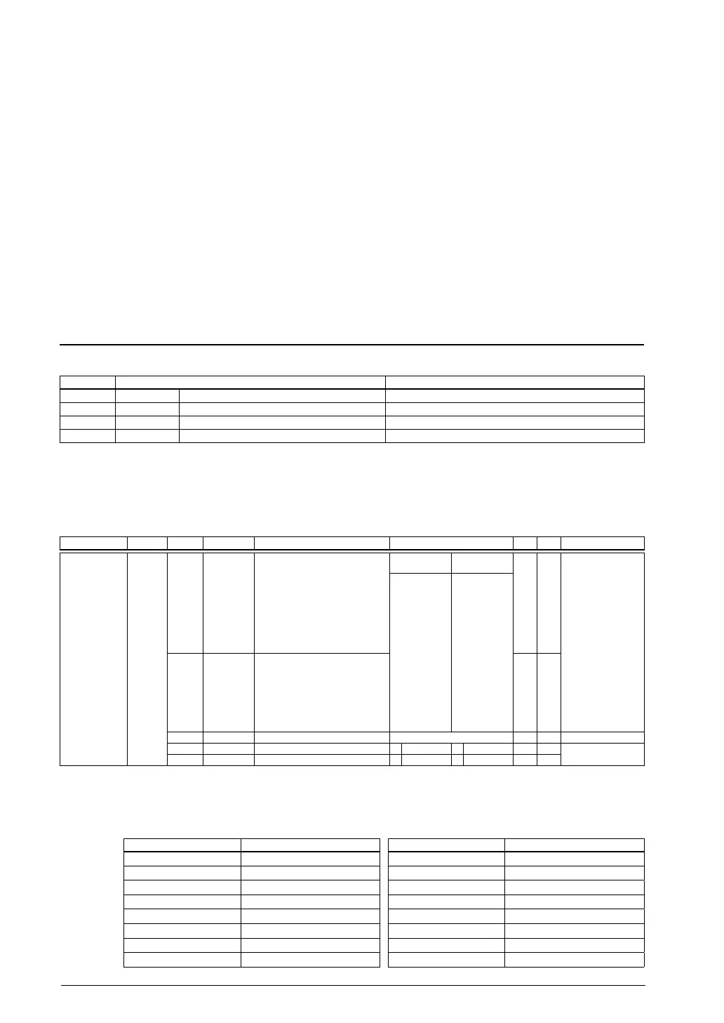
7.1 List of REMC RegistersTable 22.
Address Register name Function
0x5340 REMC_CFG REMC Configuration Register Controls the clock and data transfer.
0x5342 REMC_CAR REMC Carrier Length Setup Register Sets the carrier H/L section lengths.
0x5344 REMC_LCNT REMC Length Counter Register Sets the transmit/receive data length.
0x5346 REMC_INT REMC Interrupt Control Register Controls interrupts.
The REMC registers are described in detail below. These are 16-bit registers.
Note: When data is written to the registers, the “Reserved” bits must always be written as 0 and not 1.
REMC Configuration Register (REMC_CFG)
Register name Address Bit Name Function Setting Init. R/W Remarks
REMC
Configuration
Register
(REMC_CFG)
0x5340
(16 bits)
D15–12
CGCLK[3:0]
Carrier generator clock division
ratio select
CGCLK[3:0]
LCCLK[3:0]
Division ratio
0x0 R/W Source clock = PCLK
0xf
0xe
0xd
0xc
0xb
0xa
0x9
0x8
0x7
0x6
0x5
0x4
0x3
0x2
0x1
0x0
reserved
1/16384
1/8192
1/4096
1/2048
1/1024
1/512
1/256
1/128
1/64
1/32
1/16
1/8
1/4
1/2
1/1
D11–8
LCCLK[3:0]
Length counter clock division ratio
select
0x0 R/W
D7–2
–
reserved – – – 0 when being read.
D1
REMMD
REMC mode select
1 Receive 0 Transmit 0 R/W
D0
REMEN
REMC enable
1 Enable 0 Disable 0 R/W
D[15:12] CGCLK[3:0]: Carrier Generator Clock Division Ratio Select Bits
Selects a carrier generation clock (PCLK division ratio).
7.2 Carrier Generation Clock (PCLK Division Ratio) SelectionTable 22.
CGCLK[3:0] Division ratio CGCLK[3:0] Division ratio
0xf Reserved 0x7 1/128
0xe 1/16384 0x6 1/64
0xd 1/8192 0x5 1/32
0xc 1/4096 0x4 1/16
0xb 1/2048 0x3 1/8
0xa 1/1024 0x2 1/4
0x9 1/512 0x1 1/2
0x8 1/256 0x0 1/1
(Default: 0x0)
 Loading...