Model
5340A
Theory of Operation
4
-
1 7.
Dual
D
-
Type Edge
-
Triggered Flip
-
Flop
1820
-
0077
4
-
18.
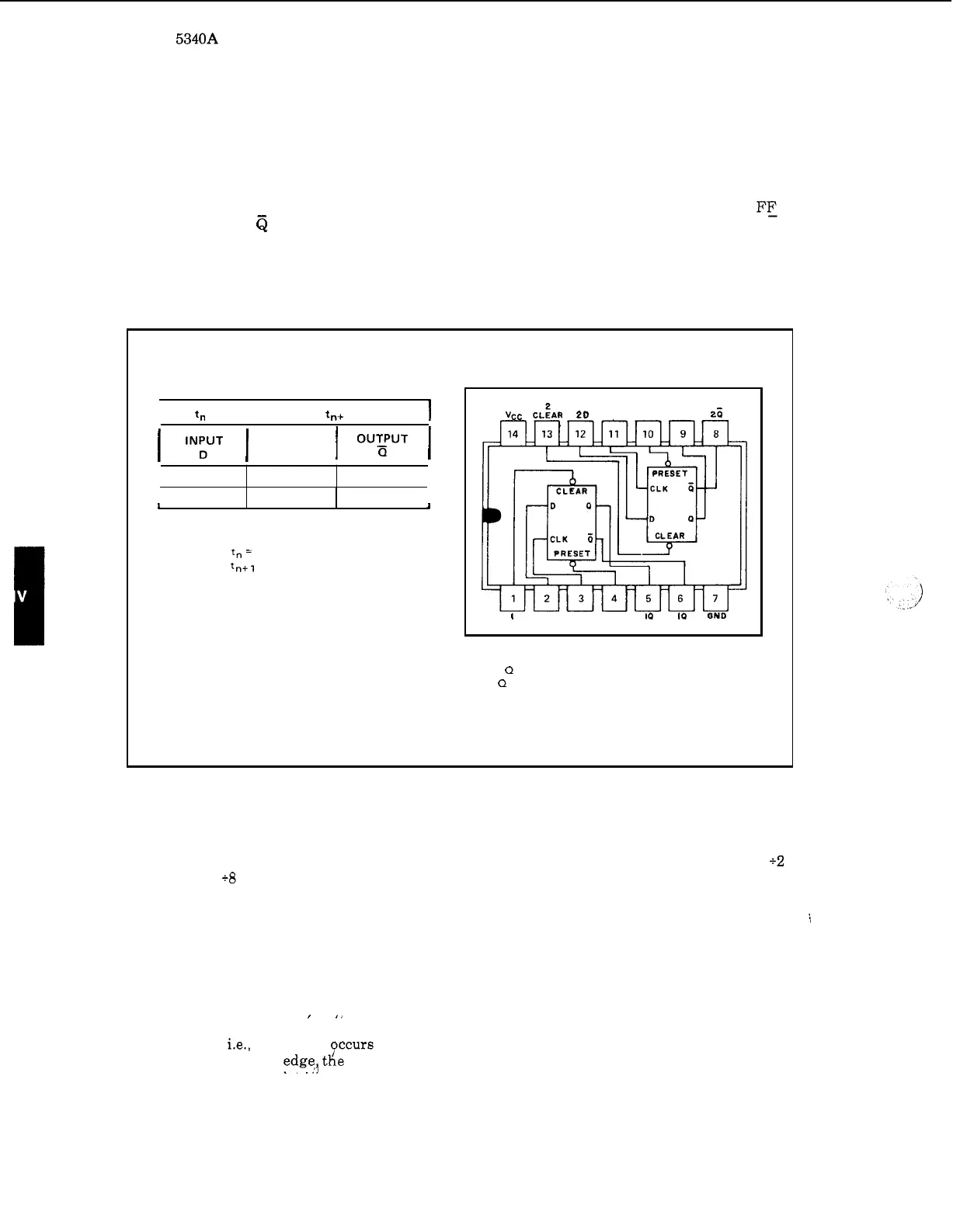
Figure
4
-
6.
shows the logic diagram, outline drawing, and truth table for the
1820
-
0077.
As the truth table shows, the input data
(D)
is
transferred to the output on the positive edge of the
clock pulse. Clock triggering
is
determined by
a
voltage level of the clock pulse and is not
directly related to the transition time of the positive going pulse. After the clock input threshold
level has been passed, the D input
is
locked out. A low
at
pin
4
or
10
will
set the respective
FF_
so
the
Q
is
high and
is
low.
A low
at
pin
1
or
13
will reset the flip
-
flop
so
that
Q
is
low and
Q
is
high. The set and reset inputs will override all other inputs.
Figure
4
-
6.
Dual D
-
Type Edge
-
Triggered Flip
-
Flop
1820
-
0077
TRUTH TABLE
(Each
Flip
-
Flop)
I
tn
I
tnc
1
1
OUTPUT
I
OUT_PUT
I
I
"yT
1
Q
.
Q
1
1
NOTES:
1.
tn
=
bit
time before clock pulse
2.
tn+l
=
bit
time after clock pulse
22
Vcc
CLEAR
2D
CLOCKPRESET
20
25
I
ID
I I
10
I0
QND
CLEAR
CLOCK
PRESET
positive logic:
Low
input
to preset sets
0
to
logical
1
Low
input
to clear sets
0
to
logical
0
Preset and clear are independent
of
clock
4
-
19. Four
-
Bit Binary Counter 1820
-
0099
4
-
20.
The binary counter (Figure
4
-
7)
consists
of
four
J
-
K
flip
-
flops connected to provide
a
+2
counter and
a
+8
counter. When pin
12
is
connected to pin
1,
the unit is
a
four
-
bit binary counter.
The input pulses are applied
at
pin
14
and simultaneous divisions of
2, 4,
8,
and
16
are available
at
the output pins
as
shown in the truth table. Thus, the counter converts the input pulses
to
an
equivalent binary output.
To
reset the counter to zero, both pins
2
and
3
must be high.
i
4
-
21. Monostable Multivibrator 1820
-
0207
4
-
22.
This
IC
(Figure
4
-
8)
contains
a
retriggerable monostable multivibrator. The inputs are dc
level sensitive,
i.e., triggering Qccurs on the rising or trailing edges of the input waveform. For
triggering on the rising
edgej the input can be applied to pins
3
and
4.
For trailing edge triggering,
pin
1
or
2
is
used. The lqgic diagram shows the input logic. When the multivibrator
is
triggered,
the
external resistor and capacitor determine the output pulse width; however, successive
inputs with
a
period shorter than the delay time
will
retrigger the multivibrator.
I
,,
4
-
6