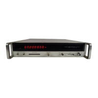
Model
5340A
Theory of Operation
4
-
186. A13 LIMITER/AMPLIFIER ASSEMBLY, 05340
-
60010
",
._
4
-
187.
Figure
8
-
19
shows the schematic diagram for
A13.
The Limiter/Amplifier input receives
the
20
MHz output of Preamplifier
No.
1
at
pin
10
and provides the necessary limiting action for
automatic amplitude discrimination.
U1
and
U2
are dual independent differential amplifiers
each containing a current source. Limiting action
is
due to current limiting in the
IC. R4, R6, R8,
and
R9
set the operating bias for the constant current source in
U1A.
L4
provides high frequency
peaking. The circuitry for
UlB, U2A,
and
U2B
is
similar to
U1A.
4
-
188. A14 LIMITER/AMPLIFIER/MIXER ASSEMBLY, 05340
-
6001 1
4
-
189.
The inputs to
A14
(Figure
8
-
20)
are the preamplifier
No.
2
signal and the
20
MHz reference
signal. The output provided by
A14
is
Fn, where Fn
=
20
kHz
N.
N
is
the harmonic multiplier of
VCO
No.
1
frequency that provides the required
20
MHz IF. The signal output of Preamplifier
No.
2
is
the result of mixing the harmonics of
F2
with the counter input signal Fx.
4
-
190.
Operational amplifier
U1
provides approximately
46
dB
of
gain for the preamplifier
signal.
U1
operates open loop to provide maximum gain.
L5, C10,
L6,
and
C12
are decoupling
networks. L7 and
C13
give bandpass filtering
at
20
MHz.
Q1
and
Q2
form
a
differential
amplifier to provide two signals out of phase to drive the mixer
(CRl-4). Q3
amplifies the
20
MHz reference signal from
A15.
The mixer detects the difference frequency between the two
input signals which
is
in range of
20
kHz to
3
MHz. The demodulator output connects to low pass
filter
L8, C19,
and
C20.
The filter rolloff point is approximately
3
MHz. Comparator
U2
has a
10%
hysteresis to discriminate against noise that could give
a
false indication of zero crossover.
The input to
U2
is
approximately
1
volt p
-
p and the
'ITL
signal output of
U2
connects to
A20
in
the counter circuits.
4
-
191 A15 10
MHz
DOUBLER ASSEMBLY, 05340
-
60012
4
-
192.
The
10
MHz Doubler (Figure
8
-
21)
receives
a
10
MHz reference from
A19,
doubles the
reference frequency to
20
MHz, and supplies two outputs. One of the
20
MHz outputs
is
used by
Phase Detector
A4
and the other
is
routed to the Limiter Amplifier/Mixer
A14.
4
-
193.
The
10
MHz reference couples through
C1
to a
10
MHz tank circuit consisting of
L1, C2,
and
C3.
The tank circuit helps to filter out noise on the reference signal. Diode
CR1
couples the
positive half cycle of the
10
MHz signal to
UlA(1)
and
CR2
couples the negative half cycle to
UlA(10).
U1A
consists of
a
differential amplifier driven by
a
current source. When the positive
half cycle of the
10
MHz drives
UlA(l),
the left side of the differential amplifier conducts and
develops
a
negative going half cycle
at
UlA(12).
Since the left half of the differential amplifier
increases conduction and a constant current source supplies the emitters of the differential
amplifier, then the right half of the differential amplifier will decrease conduction. This develops
a positive going half cycle of
UlA(11).
When
CR2
conducts, the right half of the differential
amplifier again decreases conduction and the left half increases conduction. The net result
is
a
full wave rectified signal of
20
MHz
at
UlA(12)
and
UlA(11).
C7
and
C8
couple the
20
MHz
signals to
U1B.
The operation of
U1B
is
similar to
U1A.
The signal out of the left half of
U1B
is
developed across
a
20
MHz tank circuit and coupled through
C15
to
A14.
In
a
like manner, the
output of the right half of
U1B
is coupled to
A4. Rl-C5, Rll-C9,
and
L2-C6
serve
as
filters for
the power supply voltages.
R11
lowers the collector voltage of
U1B
to meet the maximud
voltage specification for
U1.
4
-
194.
A17A1 DIRECT COUNT AMPLIFIER ASSEMBLY, 05340
-
60038
4
-
195.
This assembly (Figuke
8
-
23)
is
a
wide band analog amplifier with automatic gain control.
The input signal at
A17J1,
is
received from the sampler via A2FL1. The output, which is digital
(EECL
levels),
is
routed
tb/A22
for counting. The input
is
ac coupled through
C1
and
C2.
The
series capacitor
arrangelrient allows polarized capacitors to be used to couple ac.
I
4
-
43

 Loading...