Model
5340A
Theory of Operation
4
-
172. U2
serves as
a
summing amplifier for the phase detector output and the output of
U4.
The
gain of
U2
for the phase detector signal
is
5
as
set by
R20
and
R15.
The gain for the output of
U4
is
1
as
determined by
R20
and
R13.
The output of
U2
is
between
75
and
+13
volts and is used to
fine tune
VCO 2.
4
-
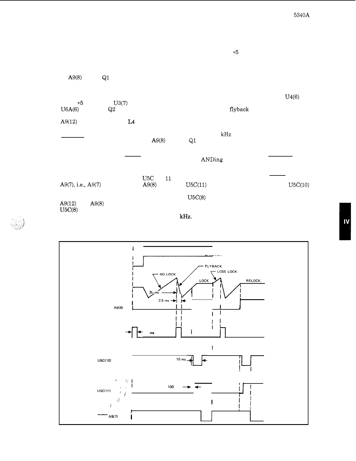
173.
The search signal
is
a
sawtooth waveform which
is
developed across
C8.
When the level
at
A9(8)
is
low,
Q1
is
off and
Q3
is on. This allows
C8
to charge through
Q3
and
R12
toward
+15
volts. The high
-
impedance tie point
is
a
teflon
-
insulated connector that prevents humidity from
discharging
C8.
The ramp developed on
C8
couples through
a
voltage follower
U4
to comparator
U3. U3
has
a
+5V
reference input
at
pin
2.
After
30
milliseconds, the ramp voltage
at
U4(6)
will
reach
+5
volts and
U3(7)
will trigger one
-
shot multivibrator
U6A
for
2.5
milliseconds.
When
U6A(6)
goes high,
Q2
turns on to discharge
C8.
This develops the flyback portion of the sawtooth,
which
lasts
for
2.5
milliseconds.
U6A
can also be triggered when the input loop lock signal
at
A9(12)
goes high.
C4
and
L4
differentiate this input into
a
spike which triggers
U6A
to discharge
C8
and
start
the transfer loop search cycle. When
a
harmonic of the
VCO
frequency beats
against the incoming Fx to produce an approximate
20
kHz
difference, the transfer loop
SEARCH
signal
goes high.
When
A9(8)
is
high,
Q1
switches on to turn
off
Q3.
This interrupts
the charging source for
C8
allowing
C8
to maintain
its
charge.
4
-
174.
The transfer loop
LOCK
signal
is
developed by ANDing the transfer loop
SEARCH
signal
an the input loop lock signal.
As
an example
of
operation, assume that the input loop
is
locked
(A9
pin
12
is
high) but the transfer loop search signal
at
A9
pin
8
is
low. Under these conditions,
U5C
pins
9
and
10
are high but
U5C
pin
11
is
low. Thus there
is
no transfer loop
LOCK
signal at
A9(7),
i.e.,
A9(7)
is high. When
A9(8)
goes high,
U5C(ll)
will go high after
100
nsec and
U5C(10)
will go high after
10
msec.
U5A
and
B
provide the
100
nsec delay and
U6B
gives the
10
msec
delay. The purpose of
U5B
and
A
is
to prevent
U5C(8)
from going low
at
the first instant that
A9(12)
and
A9(8)
are both high. This allows
U6B
to provide an overall delay of
10
msec before
U5C(8)
can go low. Thus the circuit “waits” for
10
msec
to
ensure
a
stable lock. The closed loop
bandwidth of the transfer phase lock loop
is
5
kHz.
Figure
4
-
51
shows the timing relationship of
the circuits.
Figure
4
-
51.
Transfer Loop Timing Diagram
INPUT LOOP
I
LOCK
FLYBACK
LOSE LOCK
NO
LOCK
RELOCK
RAMP SEARCH TP3
?&&pr
I
II
I
I
I
I
I
I
36mr
LJ
I
I
11
I1
I
II
25mr-WI
I
I
11
I
I1
I1
I
I
11
I
11
I
I
II
I
TP2
2
5
ms
I
I
I
I
I
I
I
I
I
I
I
I
I
I
10
rns
I
I
I
SEARCH A9181
I
II
I
J
TRANSFER LOOP
I
I
I
I
I
I
I
I
I
U5C(101
I
I
I
’
<I
,I
U5C(lll
I
4J
I
I
I
I
I
I
1l-T
II
‘I
II
I
I
I
I
I
I
I
I
I
I
I
I
I
I
!1
100
ntec
+
f
/
TRANSFER LOOP
1
LOCK A9(7l
I
-
I
4
-
41