Model 5340A
Theory
of
Operation
4
-
87. BCD to Decimal Decoder 1820
-
1047
4
-
88.
70 milliwatts.
The 1820
-
1047
is a
low power version of the 1820
-
0214.
Power dissipation
is
typically
4
-
89. Voltage Regulator 1826
-
0010
4
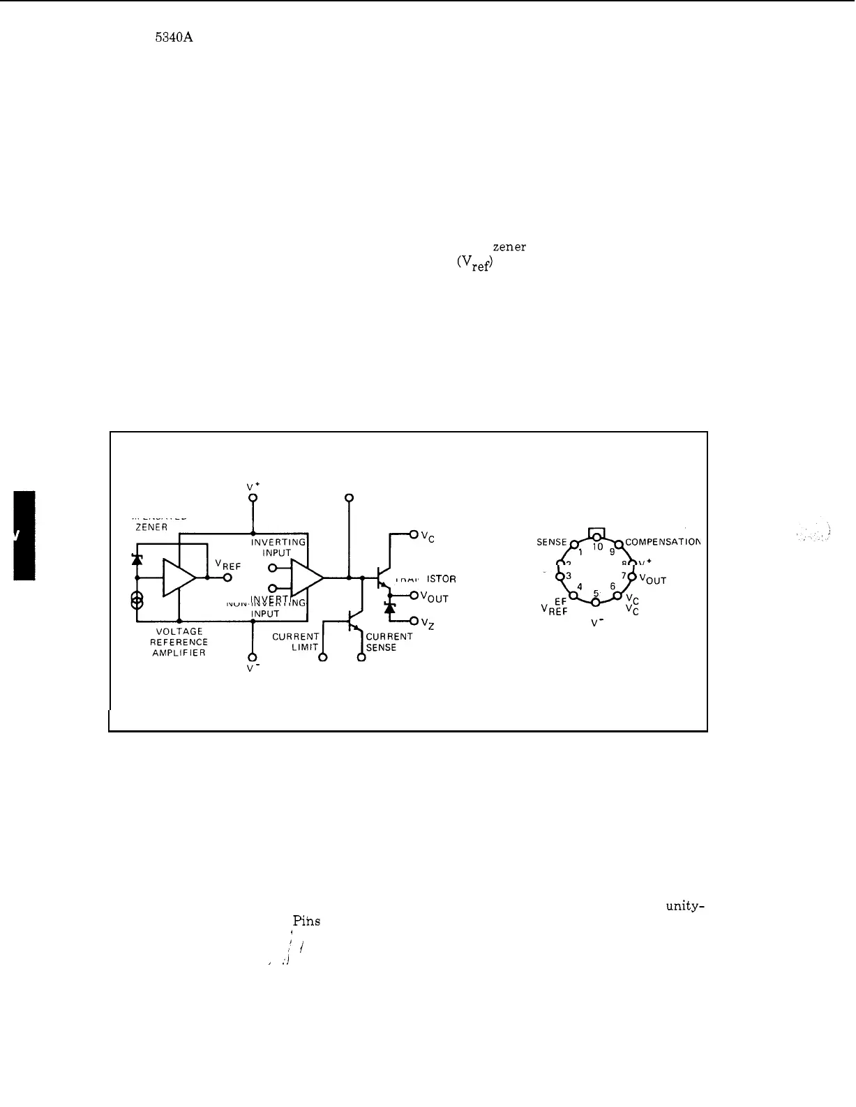
-
89. The outline drawing and equivalent circuit for the 1826
-
0010 are shown in Figure 4
-
38. The
regulator consists of
a
current source,
a
voltage reference amplifier, an error amplifier,
a
current
limiter, and
a
series pass transistor. The current source, Zener diode, and voltage reference
amplifier provide a constant 7.2 volt reference output
(Vref) for the non
-
inverting input of the
difference amplifier. The inverting input of the difference amplifier senses the power supply
output voltage through an external voltage divider.
An
example of operation
is
as
follows. If
the power supply output voltage decreases, the voltage at the inverting input (pin
2)
also
decreases. This drives the error amplifier output to bias the series pass transistor to decrease
its
impedance. When the impedance of the series pass transistor decreases, the output voltage tends
to
increase to regulate the output. The frequency compensation input prevents high frequency
oscillations.
Figure 4
-
38. Voltage Regulator 1826
-
0010
FREQUENCY
V+ COMPENSATION
TEMPERATURE
COMPENSATED
VC
SERIES PASS
TRANS
ISTO
R
NON INVERT1 'OUT
VZ
V-
ERROR CURRENT
AMPLIFIER LIMITER
CURRENT
LIMIT
CURRENT FREQUENCY
INVERTING
INPUT
NON INVERTING INPUT
uvo'.
3
VREF VC
V-
NOTE: PIN
5
CONNECTED TO CASE
4
-
91.
Voltage Regulator 1826
-
0016
4
-
92. The 1826
-
0016 (Figure 4
-
39)
is
a
negative regulator.
Operation
is
similar to the 1826
-
0010.
4
-
93. Operational Amplifier 1826
-
0021
4
-
94. The 1826
-
0021 (Figure 4
-
40)
is
an operational amplifier internally connected
as
a
unity-
gain non
-
inverting amplifier.
Pins
1
and 8 allow for offset balancing.
,
,J
j
I'i
I
4
-
28