i
I
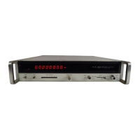
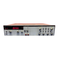
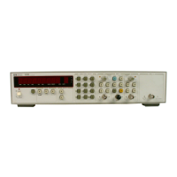
Model 5340A
Theory of Operation
4
-
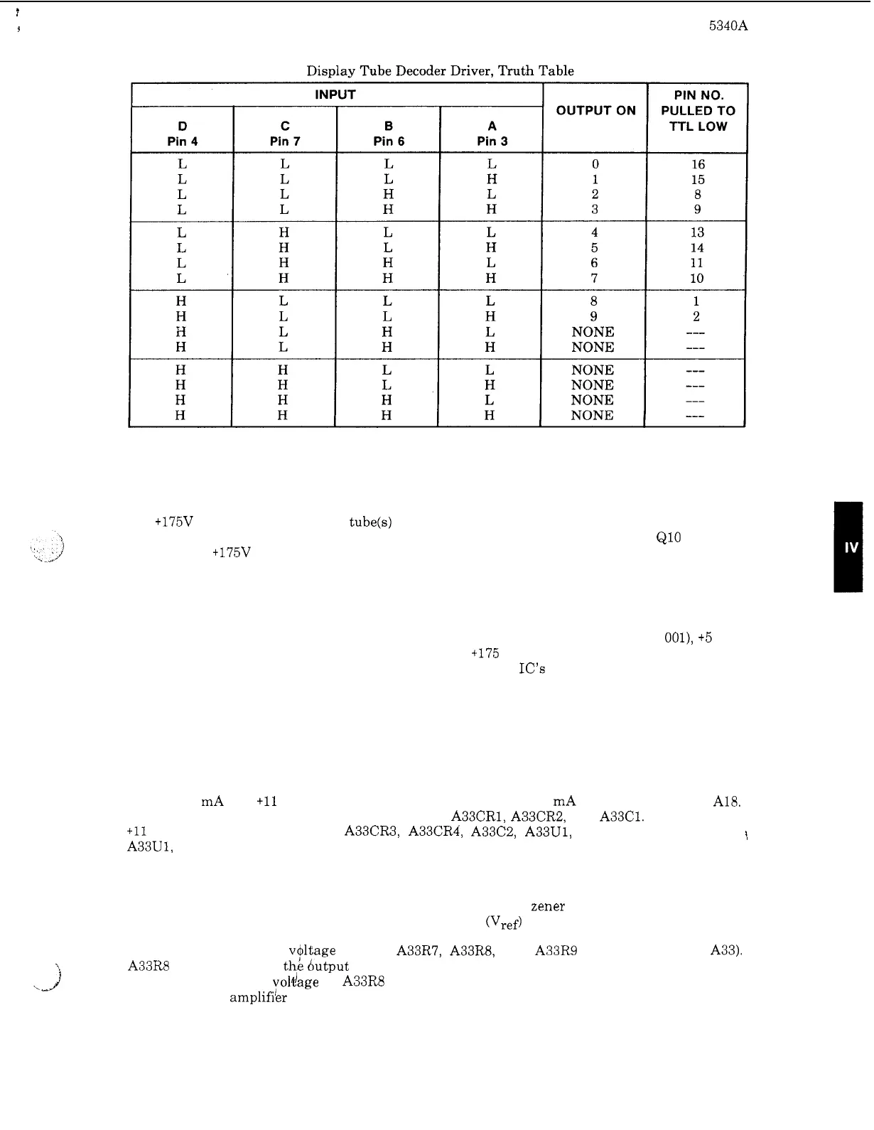
265. A26 BLANKING ASSEMBLY, 05340
-
60037
4
-
266. The Blanking Assembly (Figure 8
-
32) is controlled by logic circuits on A25 and controls
the
+175V supply to the display tube(s) that require blanking thus suppressing insignificant
zeroes. For example, with
a
TTL low on the emitter of Q5, Q5 conducts to turn on QlO which in
turn supplies
+175V to the display tube. Similarly the other four tubes are controlled.
4
-
267. POWER SUPPLIES
4
-
268. The power supplies include Time Base Power Supply A33 (part of Option
OOl),
+5 Volt
Regulator A32, +15 Volt Regulator A29,
-
15 Volt and +175 Volt Regulator A28, and
-
Volt Regu
-
lator A31.
Since the power supplies use similar regulator
IC’s and circuit arrangements, the
simplest will be described first and the applicable circuit theory will suffice for the remaining
regulator units.
4
-
269. A33 Time Base Power Supply Assembly, 05340
-
60039, (Part
of
Option
001)
4
-
270. The Time Base Power Supply (Figure 8
-
35) provides +21 volts unregulated at approxi
-
mately
100
mA and +I1 volts regulated power
at
approximately 25 mA to optional oscillator A18.
The +21 volt supply consists of full
-
wave rectifier A33CR1, A33CR2, and A33Cl. The regulated
+11
volt supply is made up of A33CR3, A33CR4, A33C2, A33U1, and associated circuitry.
1
A33U1, the voltage regulator IC has the equivalent circuit shown in Figure 4
-
52.
4
-
271. The regulator consists of
a
current source, voltage reference amplifier, error amplifier,
current limiter, and series pass transistor. The current source,
Zener diode, and voltage reference
amplifier provide a constant
7.2
volt reference output (Vref) for the noninverting input of the
difference amplifier. Th‘e inverting input of the difference amplifier senses the power supply
output voltage through
vOltage divider A33R7, A33R8, and A33R9 (see schematic for A33).
A33R8 is adjusted to set
thk
butput voltage. An example of regulation
is
as follows. If the output
voltage decreases, the
voldage
at
A33R8
and the inverting input
(Ul
pin
2)
also decreases. This
drives the error
amplifi‘er output more positive which biases the series pass transistor to decrease
its impedance. When the impedance of the series pass transistor decreases, the output voltage
tends to increase to regulate the output.
j
-.
2
4
-
51