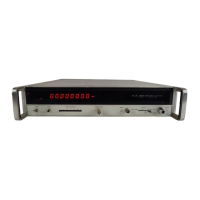
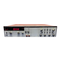
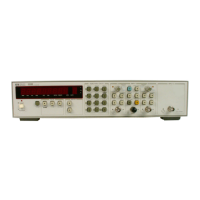
Model 5340A
Theory of Operation
D-Input
(Po, PI,
P2
or Pgl
4
-
59. Low
-
Power 4
-
Bit
Shift
Register 1820
-
0659
4
-
60.
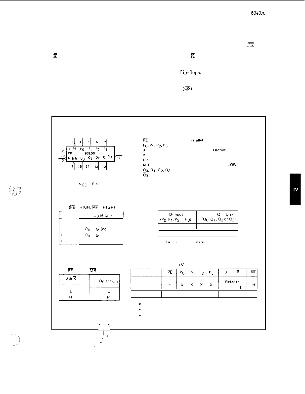
Figure 4
-
27 shows the logic diagram and pin connections for the 1820
-
0659.
A
JK
input
is
provided for the first flip
-
flop in the register. This arrangement requires
a
low to activate the
inputs together. Parallel inputs
for all four stages are
provided. These determine the next conditions of the shift register
synchronous with the clock input, whenever the parallel enable input
is
low. When the parallel
enable input
is
low, the unit appears
as
four clocked D fli?-flops. When the parallel enable
is
high, the shift register performs a one
-
bit shift for each clock input. Clocking occurs after the
low to high transistion of the clock input. Activie high outputs are provided for all four stages
and an active low output
is
also provided for the last stage
(m).
The master reset input allows all
stages to be set to zero independent of all input conditions.
input.
A
D
-
type input can be obtained by tying the
J
and
Output
0
at tnt1
IQo.
01.
02
or
E3)
Figure 4
-
27. Low
-
Power 4
-
Bit Shift Register 1820
-
0659
PIN NAMES
93LOO
K
MR
QO
91
Qz
93
Vcc
=
Pln 16
GND
=
Pin
8
TABLE
I
-
SERIAL ENTRY
(iiT
=
HIGH.MR
=
HIGH)
H
HH
TABLE
L
Qo
at
tn
(no change)
50
at
tn
(toggles)
H
-
SERIAL ENTRY
(PE
=
HIGH
,
MR
=
HIGH
)
JET
Connected
Parallel Enable (Active LOW) Input
Parallel Inputs
First Stage
J
(Active HIGH) Input
First Stage
K
(Active LOW) Input
Clock (Active HIGH Going Edge) Input
Master Reset (Active
LOW1 Input
Parallel Outputs
Complementary Last Stage Output
I
L
I
L
I
I
H
I
H
I
(ni
1
-
Indicates
sfate
after next
clock)
TABLE
IV
-
MODE SELECTION
Table
I
&
I1
Serial Entry
H
=
HIGH Voltage Level
L
=
LOW Voltage Level
X
=
Don't Care
,
:J
I
4
-
19