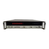
Model
5340A
Theory of Operation
4
-
136. As
shown in Figure
4
-
49,
sampling occurs
at
the zero crossing of the input signal, and the
sampler output is zero volts. When the sampler output goes positive, it indicates that the sampl
-
ing occurs later than the correct time. This generates an error signal to increase the sampling
frequency
so
that sampling occurs
at
the zero crossing. In this example, the
VCO
frequency is
exactly one
-
half the input frequency. Thus, an output frequency is obtained that is harmonically
related to the input frequency and
is
also low enough to be counted. When phase lock occurs, the
VCO
frequency
is
some fraction of the input frequency. Additional circuitry
is
needed to deter
-
mine the ratio between the input frequency and
VCO
frequency. This instrument does
NOT
use
a
DC
phase
-
lock loop, but instead uses
a
20
MHz intermediate frequency
(IF)
circuit such that
the sampler output will be exactly
20
MHz when phase lock occurs. The relationship between the
input signal and the
VCO
is:
where
N
=
Harmonic number
When phase lock occurs, the output of the sampler will be
a
20
MHz signal.
4
-
137. A1 PREAMPLIFIER ASSEMBLY
NO.
1, 05340
-
60017
4
-
138.
Preamplifiek
No.
1
(Figure
8
-
7)
consists of Sampler Driver
AlA2,
Sampler Output
AlA3,
and Preamplifier Board
AlA4. A1
receives
Fx
(
-
225
MHz to
18
GHz)
at
52
and the
VCO
signal
(
-
100
MHz to
185
MHz) at
AlA2Jl.
The Sampler Driver produces sharp rise time signals at the
VCO
frequency, which when differentiated by the sampler have usable harmonic outputs up to
the 180th order. Sampler
AlAl
consists of a thin
-
film hybrid circuit which provides high
sensitivity and wide band sampling. The Sampler Output assembly consists of
R1,
C1, C2,
and
Ll. AlA3R1
is a factory selected resistor that sets the bias on the sampler diodes in
AlA1.
AlA3Cl
and
C2
comprise
a
capacitive adding network for the output of the two sampling diodes
in
AlAl. AlA3Ll
matches impedances between the sampler output and the preamplifier input.
4
-
139.
Preamplifier Board
A1A4
consists of common emitter amplifiers
Q1
and
Q2,
two low pass
filters, and an integrated circuit
U1
which contains two independent differential amplifiers.
Overall, the amplifier provides wide band amplification from
.1
MHz to
100
MHz. Input
amplifier
Q1
is a common emitter amplfier; where
R1
and
R2
set the base bias,
R4
serves
as
the
collector load and
R3
and
C1
provide decoupling from the
+5V
supply.
R6
and
C2
give increased
high frequency gain by reducing the emitter load impedance
at
high frequencies. Two low pass
filters are included:
L1, C3-C5,
and
L3, L4, L6, C9, C11, C13,
and
C15.
These filters provide roll-
off for frequencies above
100
MHz to attenuate the
VCO
frequency.
4
-
140.
The differential amplifiers
U1A
and
U1B
provide additional gain and include high fre
-
quency peaking networks
L7
and
L9.
Resistors
R15
and
R16
set the operating bias for the
constant
-
current transistor in the
IC. L8
provides high frequency peaking for the input of
UlB.
4
-
141. A2 PREAMPLIFIER ASSEMBLY NO.
2,
05340
-
60027
4
-
142.
Preamplifier
No.
2
(Figure
8
-
8)
is similar to Preamplifier
No.
1
previously discussed.
The
assembly receives Fx at
52
and the output of
VCO No.
2
at
A2A2J1.
The output of
VCO
No.
2
is
equal to
F1
*20
kHz. The Sampler and Sampler Driver
A2A1
and
A2A2
are identical to those
used in Preamplifier
Al.
\
4
-
143.
The input circuit
on
A2A4
consists of an FET amplifier
Q1
and pnp amplifier
Q2.
The
output of
Q2
feeds through
a
low pass filter
L3, C6,
and
C7.
The filter rolls off at
60
MHz. The
circuits used for
U1A
and
U1B
are similar to those on
AlA4. A 20
MHz bandpass filter consisting
of
L8-Ll0, C20,
and
C22
is used in the output to provide an overall
8
MHz bandwidth. The fre
-
quency range for the output of preamplifier
No.
2
(FIF~)
is
16
to
24
MHz.
4
-
144. A3 HIGH-IMPEDAPCE INPUT AMPLIFIER ASSEMBLY, 05340
-
60001
4
-
145.
This assembly, (Figure
8
-
9)
receives the input signal at
54
and provides limiting for the
signal. Capacitor
C4
blocks any
DC
on the input signal.
CR5
and
CR6
are hot
-
carrier limiter
diodes that clamp the voltage on the gate of
Q1A
to
+
and
-
1.3
volts (developed across forward
biased diodes
CR1
-
CR3
and
CR2
-
CR4
respectively).
4
-
37
I,
.i

 Loading...