Model
5340A
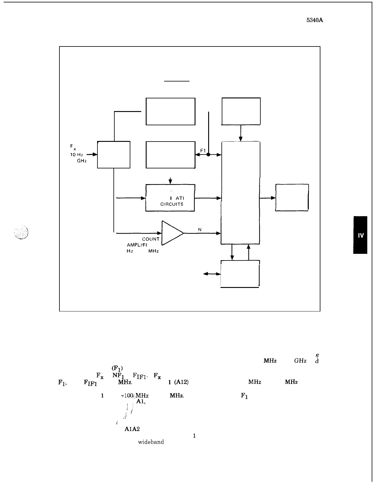
Theory of Operation
Figure
4
-
45.
Simplified Block Diagram
LOOP
AMPLIFIER
D
ETERM
I
N
AT1 ON
b
TRANSFER
~1
POWER
FX
D
ETERM
I
N
AT1 ON
PHASE LOCK
LOOP
DIVIDER
10Hz
+
-
18
GHz
A
COUNTER
CIRCUITS
4
2
+
DIRECT COUNT
AMPLl FI ER
10
HZ
-
250
MHz
DISPLAY
CIRCUITS
INTERFACE
REMOTE PROGRAMMING
(Optional)
AND DIGITAL OUTPUT CIRCUITS
I
4
-
114.
Input
Phase
Lock
Loop
4
-
115.
The input phase lock loop consists of
Al, A13, A4, A15, A6, A5, A7,
and
A12.
Overall, th
generate an output
(F1)
which is harmonically related to the input signal. This relationship is
expressed as
Fx
=
NF1
-
FIF~. F,
is
the input frequency,
N
is
the harmonic multiplier of
F1,
and
FIF~
is
20
MHz. VCO
No. 1 (A12)
operates from
-
100
MHz
to
185 MHz
and is
controlled initially by the search generator
A5.
A5
supplies
A7
with
a
triangular search signal to
drive
VCO
No. 1
from
7100,:MHz
to
185 MHz.
A12
supplies three
F1
outputs: an output to the
counter circuits, an output to
Al,
and an output to
All.
I1
purpose of the input phase lock loop
is
to accept input signals from
-
225 MHz
to
18
GHz
an
!
<I
i
.i
I
4
-
116.
harmonics up to the 180th order.
provides high sensitivity and
wideband sampling.
Sampler driver
A1A2
produces very narrow pulses
at
the
VCO
frequency with usable
Sampler
No. 1
consists of
a
thin film hybrid circuit which
4
-
33