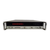
Model
5340A
Theory of Operation
4
-
175. A10
VCO
NO.
2
ASSEMBLY, 05340
-
60008
4
-
176.
When the counter is in the search phase, the
VCO
(Figure
8
-
16)
provides an output which
varies from
-
100
to
185
MHz.
When phase lock occurs, the frequency of the
VCO
is
held constant
and used by other circuitry. There are two outputs, one to the sampler driver
A2A2,
and the other
to the mixer
All.
Buffer
U1B
drives matching transformer
T1
and receives a
VCO
inhibit signal
from control board
A21.
4
-
177. U1A
is a digital device that outputs
EECL
levels but
it
is
biased in
its
active region
by
dc
feedback through low pass filter
LlO, C14,
and
R21.
The
VCO
consists of
Q5, C10, C12, L11,
CR4,
and
CR5. CR4
and
CR5
are voltage variable capacitors used to tune the
VCO
in response
to voltage variations at the collector of
Q5.
The oscillator consists of
Q5
and the resonant circuit
formed by
CR4,
which
is
capacitiire, and
L11-CR5,
which appears inductive.
C10
and
C12
form a
capacitive divider feedback path. The oscillator output
is
amplified and buffered by
Q6.
4
-
178. R17
and
R20
are current limiting resistors and
L7,
L8,
and
C13
are decoupling filters for
the two circuits. Input decoupling
is
accomplished with
a
wideband ferrite choke
Z1.
This pre
-
vents the
VCO
signal from leaking back to the input leads and interfering with other circuits.
Z1
has the property of looking resistive over
a
wide band of frequencies and appears
as
a
DC
short.
The impedance of
Z1
is
constant over the frequency range of the oscillator.
4
-
179.
Q3
is a constant current source for
Q2. CR1, R8,
and
R25
set a constant bias voltage for
Q3
to determine the value of the constant current. The emitter of
Q2
is
a
low impedance point
and the resistor networks
Rl
-
R6
and
R2-R7
are summed
at
the emitter of
Q2.
Voltage changes
at
AlO(7
and
8)
change the current through
Q2.
This varies the collector voltage of
Q2
which in
turn causes
a
voltage change
at
the emitter of
Q4
and the cathodes of
CR4
and
CR5
to change the
VCO
frequency.
Q2
has
a
nonlinear collector load to compensate for the nonlinear tuning char
-
acteristic of the
VCO.
The linearizing circuit consists
of
CR2, R5,
and
R9. As
the collector
voltage of
Q2
changes, additional load resistors are switched in by
CR2
to change the gain of the
stage.
Q4
is
an emitter follower to buffer the linearizer.
4-180. Q1
provides noise rejection for the power supply line.
If the
+15
volt supply decreases,
the current through
Q1
decreases to drop less voltage across
CR1
and
R8.
This tends to reduce
the current in
Q3
thereby increasing the voltage on the collector of
Q2
to compensate for the
decrease on the
+15V
supply. Any increase of voltage on the
+15V
supply
is
similarly com
-
pensated. The circuit is decoupled from noise on the
-
15V
supply by constant current source
Q3.
4
-
181.
L5
and
C7
constitute a lowpass filter to reduce noise generated by input amplifier
Ql-Q3.
L3-C3
and
L4-C4
provide
a
corresponding high frequency boost to maintain a flat overall
response. Filters
L1,
L2,
C1, C5, C6, L6, C9, C11, L9,
and
C16
prevent noise from being dis
-
tributed by the power supply lines.
4
-
182.
All
MIXER ASSEMBLY, 05340
-
60009
4
-
183.
The mixer (Figure
8
-
17)
receives the two
VCO
signals and provides
a
difference fre
-
quency output to Bandpass Filter/Phase Detector
A8.
Mixer
U2
is
a
differential amplifier with
a
constant current source. The signal from
VCO
No.
1
is attenuated by
R1, C4, R3
and drives the
current source. The signal from
VCO
No.
2
connects to one side of the differential amplifier
(U2
pin
12).
The other input to the differential amplifier connects to ground
(U2
pin
6).
Pin
1
of
U2
is the substrate which connects to
-
5
volts. The output of
U2
is
a
20
kHz
(nominal) square wave
output.
U1
provides
a
gain
of
22
with low response to the harmonics and supplies
a
20
kHz sine
wave at approximately
IV
p
-
p output. The power supply voltages
(+15V
and
-
5V)
are decoupled
from the power supplies by
L1,
L2,
and
C1, C2,
and
C5
through
C9.
The
20
kHz output connects
to
bandpass filter phase detector
A8.
,
I,
4
-
184. A12
VCO
NO. 1 ASSEMBLY, 05340
-
60008
4
-
185.
Figure
8
-
18
shows' the schematic diagram for
A12.
The operation of
A12
is
identical to
that of
A10.
One additional output
at
pin
5
is
used to route the
VCO
No.
1
output to
A22
for
counting.
J
4
-
42