3.1.6.4. Signals
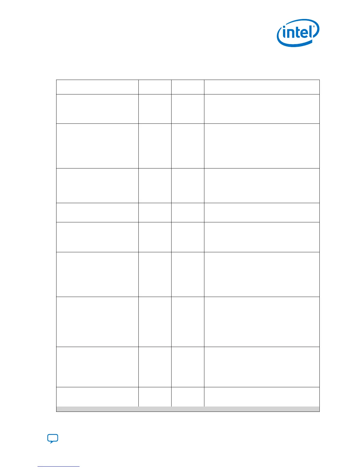
Table 22. PFL II Signals
Pin Type Weak Pull-
Up
Function
pfl_nreset
Input — Asynchronous reset for the PFL II IP core. Pull high
to enable FPGA configuration. To prevent FPGA
configuration, pull low when you do not use the PFL
II IP core. This pin does not affect the flash
programming functionality of the PFL II IP core.
pfl_flash_access_granted
Input — Used for system-level synchronization. This pin is
driven by a processor or any arbitrator that controls
access to the flash. This active-high pin is connected
permanently high if you want the PFL II IP core to
function as the flash master. Pulling the
pfl_flash_access_granted pin low prevents
the JTAG interface from accessing the flash and
FPGA configuration.
pfl_clk
Input — User input clock for the device. Frequency must
match the frequency specified in the IP core and
must not be higher than the maximum DCLK
frequency specified for the specific FPGA during
configuration. These pins are not available for the
flash programming option in the PFL II IP core.
fpga_pgm[]
Input — Determines the page for the configuration. These
pins are not available for the flash programming
option in the PFL II IP core.
fpga_conf_done
Input 10 kΩ Pull-
Up Resistor
Connects to the CONF_DONE pin of the FPGA. The
FPGA releases the pin high if the configuration is
successful. During FPGA configuration, this pin
remains low. These pins are not available for the
flash programming option in the PFL II IP core.
fpga_nstatus
Input 10 kΩ Pull-
Up Resistor
Connects to the nSTATUS pin of the FPGA. This pin
must be released high before the FPGA
configuration and must stay high throughout FPGA
configuration. If a configuration error occurs, the
FPGA pulls this pin low and the PFL II IP core stops
reading the data from the flash memory device.
These pins are not available for the flash
programming option in the PFL II IP core.
pfl_nreconfigure
Input — A low signal at this pin initiates FPGA
reconfiguration. You can reconnect this pin to a
switch for more flexibility to set this input pin high
or low to control FPGA reconfiguration. When FPGA
reconfiguration is initiated, the fpga_nconfig pin
is pulled low to reset the FPGA device. The
pfl_clk. pin registers this signal. These pins are
not available for the flash programming option in
the PFL II IP core.
pfl_flash_access_request
Output — Used for system-level synchronization. When
necessary, this pin connects to a processor or an
arbitrator. The PFL II IP core drives this pin high
when the JTAG interface accesses the flash or the
PFL II IP core configures the FPGA. This output pin
works in conjunction with the flash_noe and
flash_nwe pins.
flash_addr[]
Output — Address inputs for memory addresses. The width of
the address bus line depends on the density of the
flash memory device and the width of the
continued...
3. Intel Stratix 10 Configuration Schemes
UG-S10CONFIG | 2018.11.02
Send Feedback
Intel Stratix 10 Configuration User Guide
49
 Loading...