Point Grey Flea3 USB 3.0 Technical Reference 4 Input/Output Control
Determine Strobe Support
The next step is to determine whether our desired strobe pin, GPIO2, is capable of outputting a strobe signal. To do
this, get the value of the appropriate STROBE_ x_ INQ register (page 47); in this case, the STROBE_ 0_ INQ register
0x1408. Assuming we have correctly configured GPIO2 to be an output, we should get a value of:
8 E 0 0 0 F F F Hex
1000 1110 0000 0000 0000 1111 1111 1111 Binary
0-7 8-15 16-23 24-31 Bits
Bit 0 is a ‘1’, which confirms that the strobe functionality is present on this GPIO pin. Bit 4 points to the ability to read
the value of this feature. Bit 5 indicates the ability to turn the strobe on and off, and bit 6 indicates that we can change
the strobe signal polarity. Bits 8-19 are ‘0’, which means the minimum strobe duration is zero. Bits 20-31 are ‘0xFFF’ or
4096 in decimal, so the maximum strobe delay and duration is 4096.
Configure the Desired Pin to Output a Strobe
At this point, GPIO2 is set as an output pin and we know it can be a strobe signal source. Now, we need to enable it as
a strobe source by “turning it on” using the GPIO pin’s STROBE_x_CNT register (page 47).
Continuing our example, the desired strobe pin is GPIO2. Therefore, we want to look at the STROBE_2_CNT register
0x1508. The values that we enter in the Delay_Value and Duration_ Value fields of this register are determined as
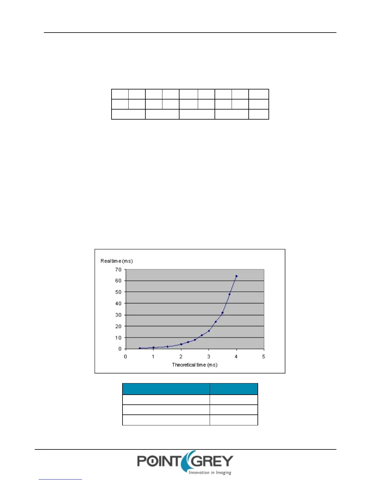
follows: for values up to approximately 0x400 (1024 decimal), each value increment is a tick of a 1.024MHz clock.
Values between 0x401 and 0xFF become non-linear in the manner shown in the figure below:
Duration_Value/Delay_Value Real Time (ms)
0x050 0.078
0x200 0.5
0x400 1
Revised 9/27/2012
Copyright ©2011-2012 Point Grey Research Inc.
45