13. Timer S
puorG92/C61M
page 152
854fo7002,03.raM21.1.veR
2110-1010B90JER
Table 13.3 Base Timer Associated Register Settings (Time Measurement Function, Waveform
Generation Function, Communication Function)
Register Bit Function
G1BCR0 BCK1 to BCK0 Select a count source
RST4 Select base timer reset timing
IT Select the base timer overflow
G1BCR1 RST2 to RST1 Select base timer reset timing
BTS Used to start the base timer
UD1 to UD0 Select how to count
G1BT - Read or write base timer value
G1DV - Divide ratio of a count source
Set the following registers to set the RST1 bit to 1 (base timer reset by matching the base timer with the G1PO0 register)
G1POCR0 MOD1 to MOD0 Set to 002 (single-phase waveform output mode)
G1PO0 - Set reset cycle
G1FS FSC0 Set to 0 (waveform generating function)
G1FE IFE0 Set to 1 (channel operation start)
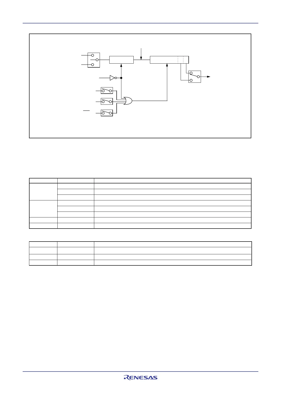
Figure 13.11 Base Timer Block Diagram
(n+1) divider
RST4
RST1
RST2
Matched with G1BTRR
Matched with G1PO0 register
Base timer
b14 b15
Base timer
overflow request
BCK1 to BCK0
IT
BTS bit in G1BCR1 register
Two-phase pulse input
Overflow signal
Input "L" to INT1 pin
Base timer reset
11
10
0
1
fBT1
NOTE:
1. Divider is reset when the BTS bit is set to 0.
IT, RST4, BCK1 to BCK0: Bits in the G1BCR0 register
RST2 to RST1: Bits in the G1BCR1 register
(Note 1)
f
1
or f
2
 Loading...


