14.Serial I/O
puorG92/C61M
page 186
854fo7002,03.raM21.1.veR
2110-1010B90JER
14.1.1.4 Continuous receive mode
When the UiRRM bit (i=0 to 2) is set to 1 (continuous receive mode), the TI bit in the UiC1 register is
set to 0 (data present in the UiTB register) by reading the UiRB register. In this case, i.e., UiRRM bit is
set to 1, do not write dummy data to the UiTB register in a program. The U0RRM and U1RRM bits are
the bit 2 and bit 3 in the UCON register, respectively, and the U2RRM bit is the bit 5 in the U2C1
register.
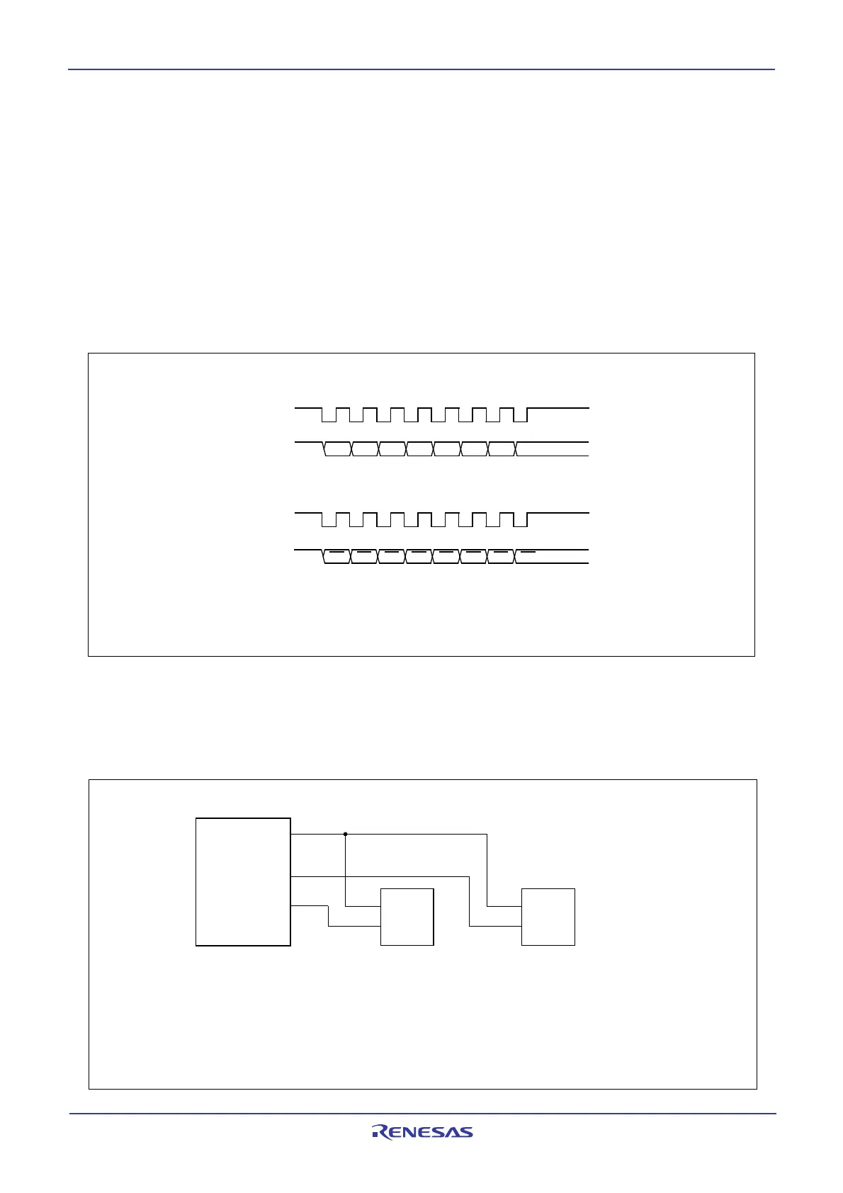
14.1.1.5 Serial data logic switch function (UART2)
When the U2LCH bit in the U2C1 register is set to 1 (reverse), the data written to the U2TB register
has its logic reversed before being transmitted. Similarly, the received data has its logic reversed
when read from the U2RB register. Figure 14.13 shows serial data logic.
Figure 14.13 Serial data logic switch timing
14.1.1.6 Transfer clock output from multiple pins function (UART1)
The CLKMD1 to CLKMD0 bits in the UCON register can choose one from two transfer clock output
pins. (See Figure 14.14) This function is valid when the internal clock is selected for UART1.
Figure 14.14 Transfer Clock Output From Multiple Pins
D0 D1 D2 D3 D4 D5 D6 D7
Transfer clock
TxD
2
(no reverse)
“H”
“L”
“H”
“L”
TxD2
(reverse)
D0 D1 D2 D3 D4 D5 D6 D7
“H”
“L”
(1) When the U2LCH bit in the U2C1 register is set to 0 (no reverse)
Transfer clock
“H”
“L”
(2) When the U2LCH bit in the U2C1 register is set to 1 (reverse)
NOTE:
1. This applies to the case where the CKPOL bit in the U2C0 register is set to 0 (transmit data
output at the falling edge and the receive data taken in at the rising edge of the transfer
clock) and the UFORM bit is set to 0 (LSB first).
MCU
TXD1 (P67)
CLKS
1 (P64)
CLK
1 (P65)
IN
CLK
IN
CLK
Transfer enabled
when the CLKMD0
bit in the UCON
register is set to 0
Transfer enabled
when the CLKMD0
bit in the UCON
register is set to 1
NOTES:
1. This applies to the case where the CKDIR bit in the U1MRregister is set to 0 (internal clock) and
the CLKMD1 bit in the UCON register is set to 1 (transfer clock output from multiple pins).
2. This applies to the case where U1MAP bit in PACR register is set to 0 (P6
7 to P64).
 Loading...


