14. Serial I/O
puorG92/C61M
page 185
854fo7002,03.raM21.1.veR
2110-1010B90JER
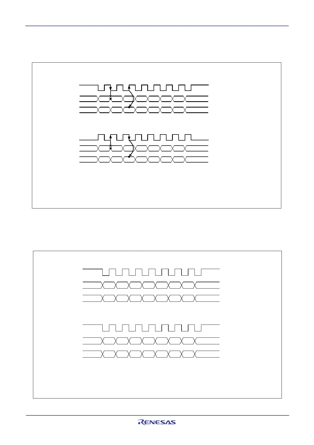
14.1.1.2 CLK Polarity Select Function
Use the CKPOL bit in the UiC0 register (i=0 to 2) to select the transfer clock polarity. Figure 14.11
shows the polarity of the transfer clock.
Figure 14.11 Polarity of transfer clock
14.1.1.3 LSB First/MSB First Select Function
Use the UFORM bit in the UiC0 register (i=0 to 2) to select the transfer format. Figure 14.12 shows
the transfer format.
Figure 14.12 Transfer format
(2) When the CKPOL bit in the UiC0 register is set to 1 (transmit data output at the rising
edge and the receive data taken in at the falling edge of the transfer clock)
D
1
D
2
D
3
D
4
D
5
D
6
D
7
D
1
D
2
D
3
D
4
D
5
D
6
D
7
D
0
D
0
T
X
D
i
R
X
D
i
CLK
i
(1) When the CKPOL bit in the UiC0 register is set to 0 (transmit data output at the falling edge
and the receive data taken in at the rising edge of the transfer clock)
D
1
D
2
D
3
D
4
D
5
D
6
D
7
D0
D
1
D
2
D
3
D
4
D
5
D
6
D
7
D
0
T
X
D
i
R
X
D
i
CLK
i
(2)
(3)
i = 0 to 2
NOTES:
1. This applies to the case where the UFORM bit in the UiC0 register is set to 0 (LSB first) and the
UiLCH bit in the UiC1 register is set to 0 (no reverse).
2. When not transferring, the CLKi pin outputs a high signal.
(1) When the UFORM bit in the UiC0 register 0 (LSB first)
D0
D0
D1 D2 D3 D4 D5 D6 D7
D1 D2 D3 D4 D5 D6 D7
TXDi
RXDi
CLKi
(2) When the UFORM bit in the UiC0 register is set to 1 (MSB first)
D6 D5 D4 D3 D2 D1 D0
D7
D7
D6 D5 D4 D3 D2 D1 D0
TXDi
RXDi
CLKi
i = 0 to 2
NOTE:
1. This applies to the case where the CKPOL bit in the UiC0 register is set to 0 (transmit data output at
the falling edge and the receive data taken in at the rising edge of the transfer clock) and the
UiLCH bit in the UiC1 register 0 (no reverse).
 Loading...


