15. A/D Converter
puorG92/C61M
page 227
854fo7002,03.raM21.1.veR
2110-1010B90JER
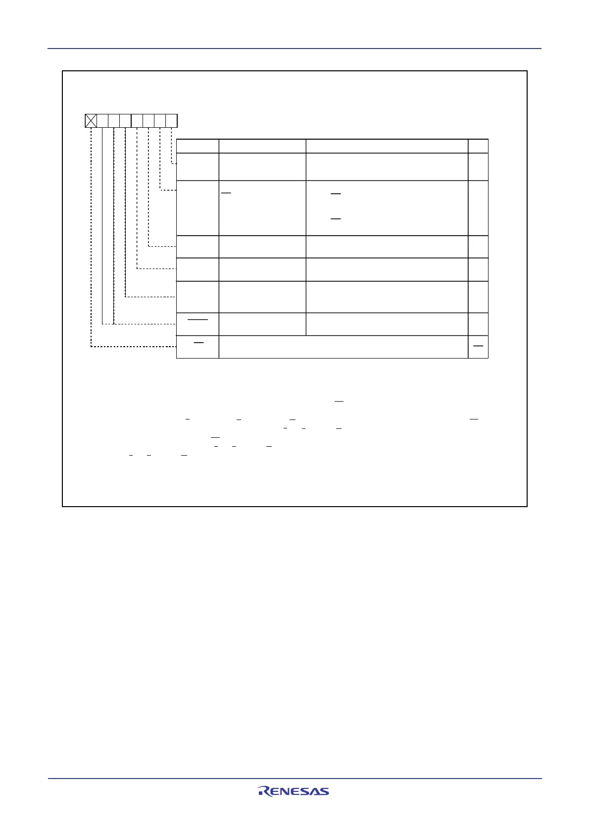
Figure 15.5 TB2SC Register
PWCON
Symbol Address
TB2SC 039E
16
X0000000
2
Timer B2 reload timing
switch bit
0: Timer B2 underflow
1: Timer A output at odd-numbered
Timer B2 special mode register
(1)
Bit Name FunctionBit Symbol
b7 b6 b5 b4 b3 b2 b1 b0
IVPCR1
Three-phase output port
SD control bit 1
0: Three-phase output forcible cutoff
by SD pin input (high impedance)
disabled
1: Three-phase output forcible cutoff
by SD pin input (high impedance)
enabled
RW
RW
RW
Nothing is assigned. If necessary, set to 0.
When read, its content is 0
(b7)
TB2SEL
Trigger select bit
0: TB2 interrupt
1: Underflow of TB2 interrupt
generation frequency setting counter [ICTB2]
RW
RW
TB0EN
Timer B0 operation mode
select bit
0: Other than A/D trigger mode
1: A/D trigger mode
RW
TB1EN
Timer B1 operation mode
select bit
0: Other than A/D trigger mode
1: A/D trigger mode
RW
(2)
(3, 4, 7)
(5)
(5)
(6)
(b6-b5)
Reserved bits
Set to 0
00
After Reset
NOTES:
1. Write to this register after setting the PRC1 bit in the PRCR register to 1 (write enabled).
2. If the INV11 bit is 0 (three-phase mode 0) or the INV06 bit is 1 (triangular wave modulation mode), set this bit to 0 (timer
B2 underflow).
3. When setting the IVPCR1 bit to 1 (three-phase output forcible cutoff by SD pin input enabled), Set the PD8
5
bit to 0 (= input
mode).
4. Related pins are U(P8
0
), U(P8
1
), V(P7
2
), V(P7
3
), W(P7
4
), W(P7
5
). When a high-level ("H") signal is applied to the SD pin
and set the IVPCR1 bit to 0 after forcible cutoff, pins U, U, V, V, W, and W are exit from the high-impedance state. If a low-
level (“L”) signal is applied to the SD pin, three-phase motor control timer output will be disabled (INV03=0). At this time,
when the IVPCR1 bit is 0, pins U, U, V, V, W, and W become programmable I/O ports. When the IVPCR1 bit is set to 1,
pins U, U, V, V, W, and W are placed in a high-impedance state regardless of which function of those pins is used.
5. When this bit is used in delayed trigger mode 0, set bits TB0EN and TB1EN to 1 (A/D trigger mode).
6. When setting the TB2SEL bit to 1 (underflow of TB2 interrupt generation frequency setting counter[ICTB2]), set the INV02
bit to 1 (three-phase motor control timer function).
 Loading...


