15. A/D Converter
puorG92/C61M
page 226
854fo7002,03.raM21.1.veR
2110-1010B90JER
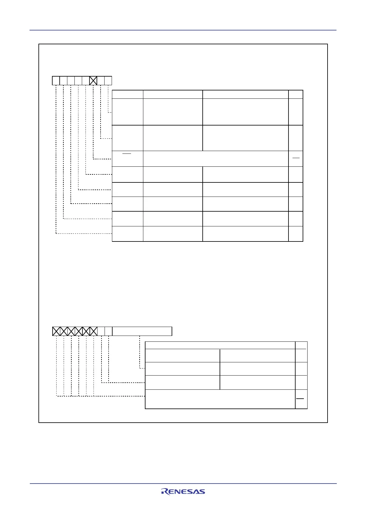
Figure 15.4 ADSTAT0 Register and AD0 to AD7 Registers
A/D Register i (i=0 to 7)
Symbol Address After Reset
AD0 03C1
16
to 03C0
16
Undefined
AD1 03C3
16
to 03C2
16
Undefined
AD2
03C5
16
to 03C4
16
Undefined
AD3
03C7
16
to 03C6
16
Undefined
AD4
03C9
16
to 03C8
16
Undefined
AD5
03CB
16
to 03CA
16
Undefined
AD6
03CD
16
to 03CC
16
Undefined
AD7
03CF
16
to 03CE
16
Undefined
Eight low-order bits of
A/D conversion result
Function
(b15)
b7b7 b0 b0
(b8)
When the BITS bit in the ADCON1
register is 1 (10-bit mode)
Nothing is assigned. If necessary, set to 0.
When read, its content is 0
When read, its content is
undefined
RW
RO
RO
Two high-order bits of
A/D conversion result
When the BITS bit in the ADCON1
register is 0 (8-bit mode)
A/D conversion result
A/D Conversion Status Register 0
(1)
Symbol Address After reset
ADSTAT0 03D3
16
00
16
b7 b6 b5 b4 b3 b2 b1 b0
AN1 trigger status flag
0: AN1 trigger did not occur during
AN0 conversion
1: AN1 trigger occured during
AN0 conversion
Bit Symbol Bit Name Function RW
ADERR0
Conversion termination fla
g
AN0 conversion status flag
ADSTT0
ADERR1
ADTCSF
RW
RO
RW
RO
RO
Nothing is assigned. If necessary, set to 0.
When read, its content is 0
(b2)
ADSTRT0
AN0 conversion
completion status fla
g
0: Conversion not terminated
1: Conversion terminated by
Timer B0 underflo
w
Delayed trigger sweep
status flag
0: Sweep not in progress
1: Sweep in progress
0: AN0 conversion not in progress
1: AN0 conversion in progress
ADSTT1
RW
0: AN0 conversion not completed
1: AN0 conversion completed
ADSTRT1
RW
AN1 conversion status flag
0: AN1 conversion not in progress
1: AN1 conversion in progress
AN1 conversion
completion status flag
0: AN1 conversion not completed
1: AN1 conversion completed
NOTE:
1. ADSTAT0 register is valid only when the DTE bit in the ADTRGCON register is set to 1.
RW
 Loading...


