15. A/D Converter
puorG92/C61M
page 243
854fo7002,03.raM21.1.veR
2110-1010B90JER
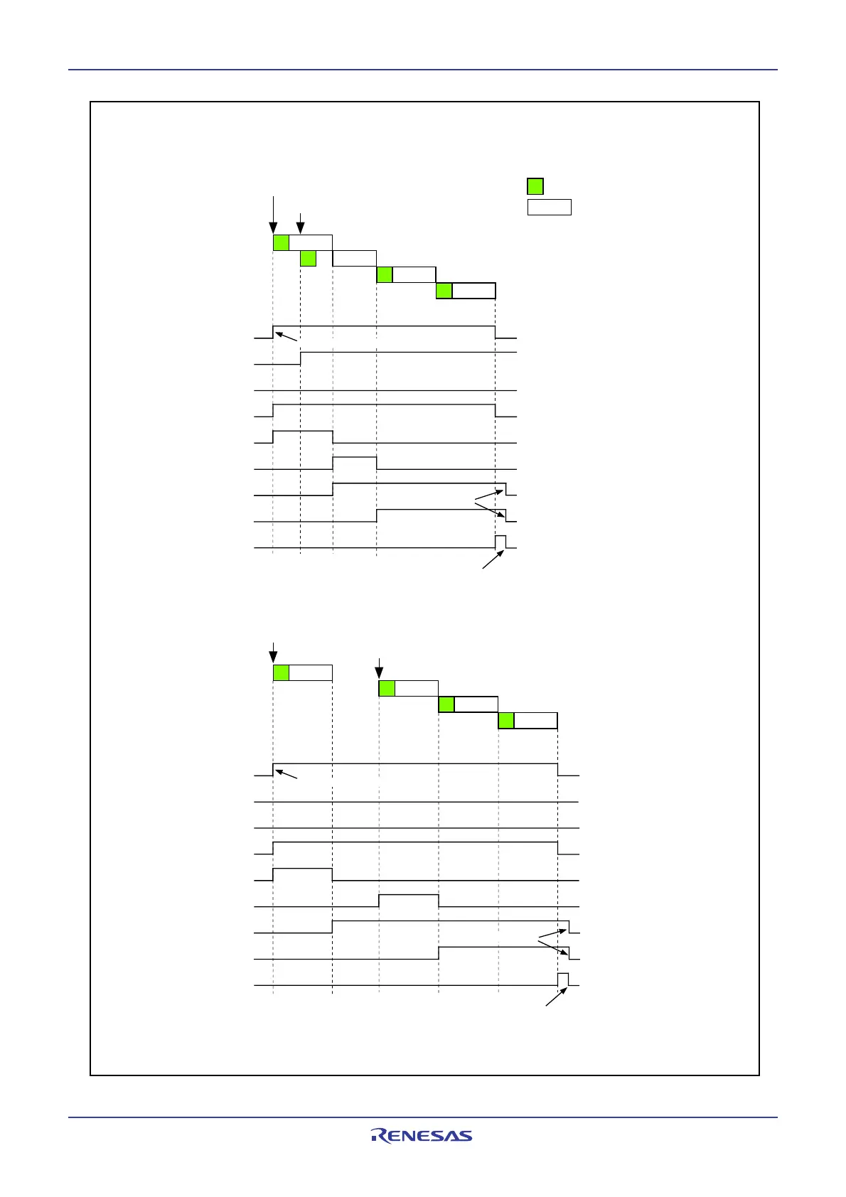
Figure 15.20 Each Flag Operation in ADSTAT0 Register Associated with the Operation
Example in Delayed Trigger Mode 0 (1)
AN
0
AN
1
AN
2
AN
3
Timer B0 underflow
1
0
1
0
1
0
1
0
1
0
1
0
1
0
1
0
1
0
AN
0
AN
1
AN
2
AN
3
1
0
1
0
1
0
1
0
1
0
1
0
1
0
1
0
1
0
A/D pin input
voltage sampling
A/D pin conversion
Do not set to 1 by program
Do not set to 1 by program
Set to 0 by an interrupt request acknowledgement or a program
Set to 0 by an interrupt request acknowledgement or a program
Set to 0 by program
Set to 0 by program
ADST flag: Bit 6 in the ADCON0 register
ADERR0
ADERR1
ADTCSF
ADSTT0
ADSTT1
ADSTRT0 and ADSTRT1 fla
: bits 0
1
3
4
5
6 and 7 in the ADSTAT0 re
ister
ADST flag
ADERR0 flag
ADERR1 flag
ADTCSF flag
ADSTT0 flag
ADSTT1 flag
ADSTRT0 flag
ADSTRT1 flag
IR bit in the ADIC
register
ADST flag
ADERR0 flag
ADERR1 flag
ADTCSF flag
ADSTT0 flag
ADSTT1 flag
ADSTRT0 flag
ADSTRT1 flag
IR bit in the ADIC
register
Timer B0 underflow
Timer B1 underflow
Timer B1 underflow
•Example when selecting AN
0
to AN
3
to A/D sweep pins (SCAN1 to SCAN0 = 01
2
)
•Example 1: When Timer B1 underflow is generated during AN
0
pin conversion
•Example 2: When Timer B1 underflow is generated after AN
0
pin conversion
 Loading...


