16. MULTI-MASTER I
2
C bus INTERFACE
puorG92/C61M
page 258
854fo7002,03.raM21.1.veR
2110-1010B90JER
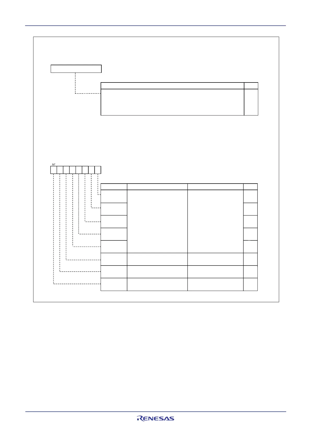
Figure 16.3 S00 and S20 Registers
0: Standard clock mode
1: High-speed clock mode
0: ACK is returned
1: ACK is not returned
0: No ACK clock
1: With ACK clock
ACK Clock Bit
ACK Bit
S
CL Mode Specification Bit
S
CL Frequency Control Bits
CCR0
CCR1
CCR2
CCR3
CCR4
FAST
MODE
ACKBIT
ACK-CLK
FunctionBit NameBit Symbol
00
16
After Reset
02E4
16
AddressSymbol
S20
b7
4
b2 b1 b0
0
lock
ontrol Re
ister
2
RW
See Table 16.3
RW
RW
RW
RW
RW
RW
RW
RW
Symbol Address After Reset
S00 02E0
16
XX
16
b
7b
6b
5b
4b
3b
2b
1b
0
RWFunction
RW
(
1
)
NOTE:
1. Write is enabled only when the ES0 bit in the S1D0 register is 1 (I
2
C bus interface is enabled). Write the transmit data after
the receive data is read because the S00 register is used to store both the transmit and receive data. When the S00 register
is set, bits BC2 to BC0 in the S1D0 register are set to 000
2
, while bits LRB, AAS, and AL in the S10 register are set to 0
respectively.
Transmit/receive data are stored.
In master transmit mode, the start condition/stop condition are triggered by writing data
to the register (refer to 16.9 START Condition Generation Method and 16.11 STOP
Condition Generation Method). Start transmitting/receiving data while synchronizing
with S
CL
I
2
C0 Data Shift Register
 Loading...


