20. Flash Memory Version
puorG92/C61M
page 344
854fo7002,03.raM21.1.veR
2110-1010B90JER
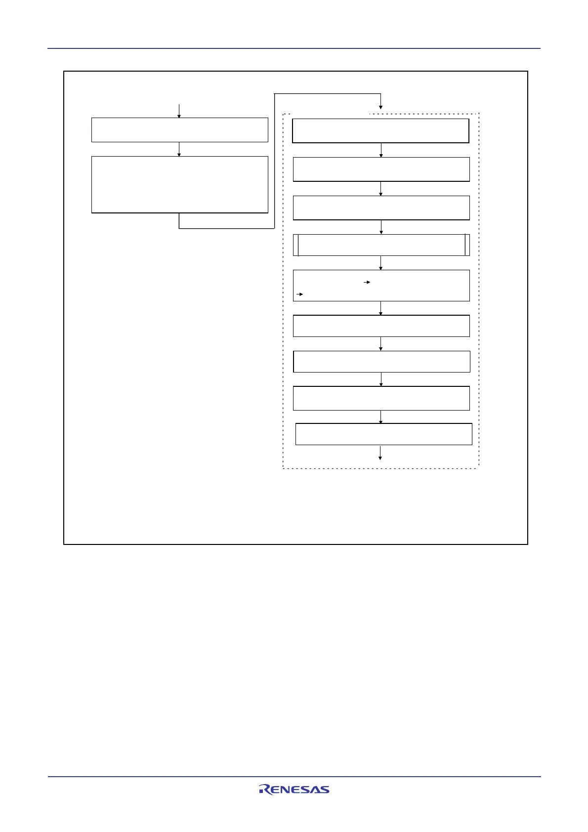
Figure 20.10 Processing Before and After Low Power Dissipation Mode
Start main clock
oscillation
Transfer a low power internal consumption mode
program to RAM area
Switch the clock source of CPU clock.
Turn main clock off
(2)
Jump to the low power consumption mode
program transferred to internal RAM area.
(In the following steps, use the low-power
consumption mode program or internal RAM area)
Wait until the flash memory circuit stabilizes (tps)
(3)
Set the FMSTP bit to 0 (flash memory operation)
Set the FMSTP bit to 1 (flash memory stopped.
Low power consumption state)
(1)
Process of low power consumption mode or
on-chip oscillator low power consumption mode
switch the clock source of the CPU clock
(2)
Low power consumption
mode program
Set the FMR01 bit to 0
(CPU rewrite mode disabled)
Set the FMR01 bit to 1 after setting 0 (CPU
rewrite mode enabled)
(2)
Jump to a desired address in the flash memory
wait until oscillation stabilizes
NOTES:
1. Set the FMRSTP bit to 1 after setting the FMR01 bit to 1 (CPU rewrite mode).
2. Wait until the clock stabilizes to switch the clock source of the CPU clock to the main clock or the sub clock.
3. Add a tps wait time by a program. Do not access the flash memory during this wait time.
 Loading...


